
Eureka
For R&D, Eureka makes reading and utilizing patents & technical documents easy.
Eureka AIR
Designed for self-driven R&D workflows. Generate viable solutions, solve complex R&D challenges, empower your innovation with AI.

Eureka Materials
Designed for material experts only. Revolutionize your material R&D, from search, analyze, to developing new materials.

TechResearch
Generate reliable direction feasibility study reports for your R&D in just a few steps.

TechSeek
Discover and master advanced knowledge NOW. Basics, ideas, possibilities, all at once.

TechMind
As an expert in R&D Theories, TechMind can generates customized viable solutions instantly.

TechRisk
Analyze your overall solution with one click, know your potential R&D risks in advance.

TechMonitor
Get weekly tech updates, stay abreast of the latest tech innovations and key insights.
Electronic element mounting substrate and electronic device
- Summary
- Abstract
- Description
- Claims
- Application Information
AI Technical Summary
Benefits of technology
Problems solved by technology
Method used
Image

Examples
first embodiment
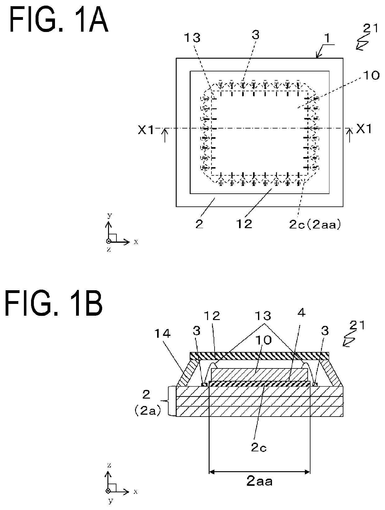
[0023]An electronic device 21 and the electronic element mounting substrate 1 according to the first embodiment of the present disclosure will be described with reference to FIGS. 1 and 2.
[0024]The substrate 2a of the electronic element mounting substrate 1 includes a first substrate portion 2d and a second substrate portion 2e. The second substrate portion 2e is located on an upper surface 2da of the first substrate portion 2d. The second substrate portion 2e is located at a section corresponding to the first protrusion portion 2aa and / or the second protrusion portion 2ab. The second substrate portion 2e may include a plurality of insulating layers. For example, in a case where the substrate 2a includes at least the first protrusion portion 2aa, the second substrate portion 2e includes at least one (one layer of) insulating layer 2c including the mounting region 4 where an electronic element 10 is mounted on an upper surface. The substrate 2a includes the plurality of electrode pad...
second embodiment
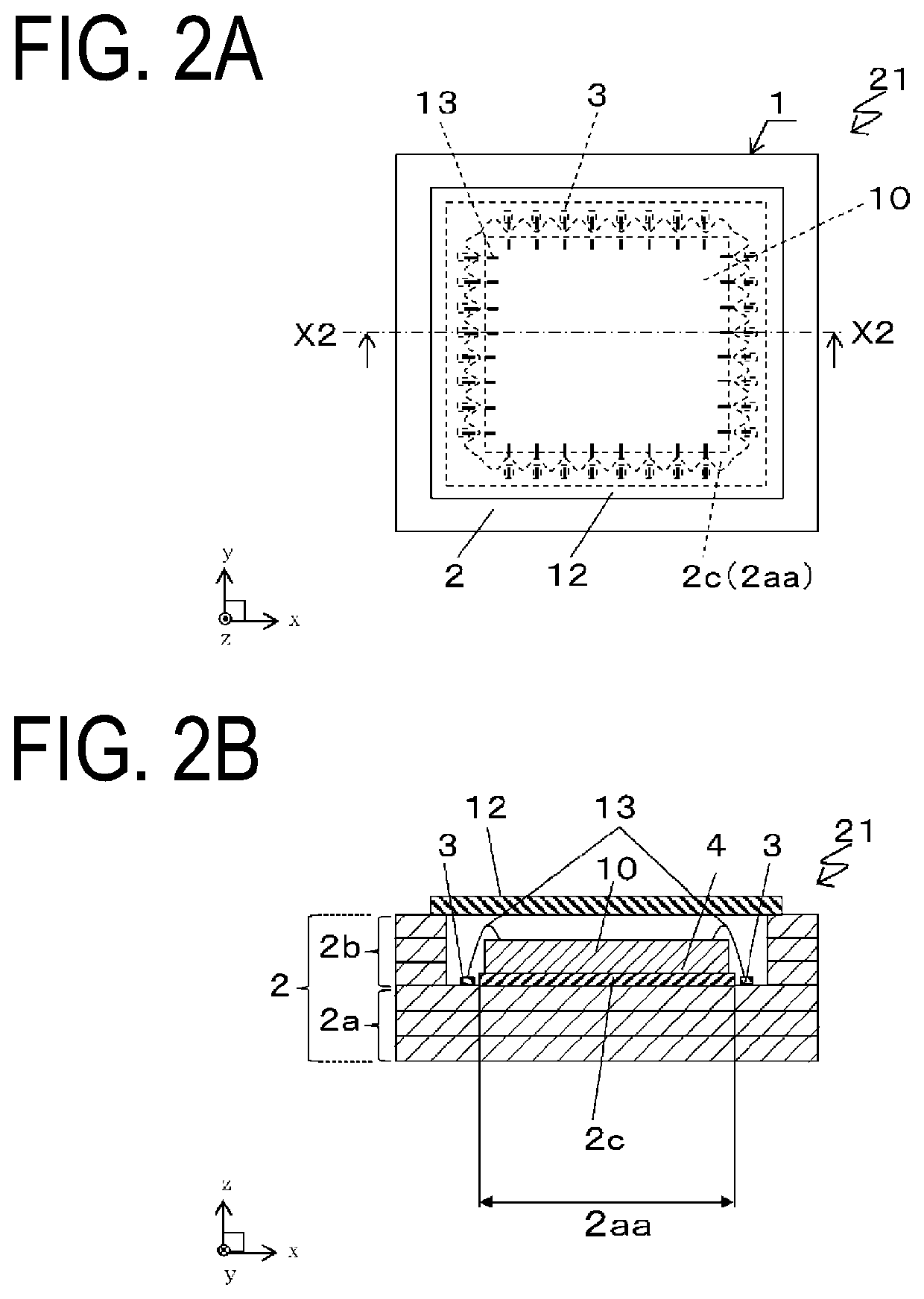
[0064]The electronic device 21 and the electronic element mounting substrate 1 according to the second embodiment of the present disclosure will be described with reference to FIG. 3.
[0065]As in the first embodiment, the substrate 2a of the electronic element mounting substrate 1 may include the first substrate portion 2d and the second substrate portion 2e. The second substrate portion 2e is located on the upper surface 2da, which is an upper surface of the first substrate portion 2d. The second substrate portion 2e is located at a section corresponding to the first protrusion portion 2aa and / or the second protrusion portion 2ab. The second substrate portion 2e may include a plurality of insulating layers. The substrate 2a including the mounting region 4 includes the plurality of electrodes 3 (electrode pads 3) located on an upper surface of the substrate 2a and around the mounting region 4 in a top view. In this example, the substrate 2a includes at least the second protrusion por...
third embodiment
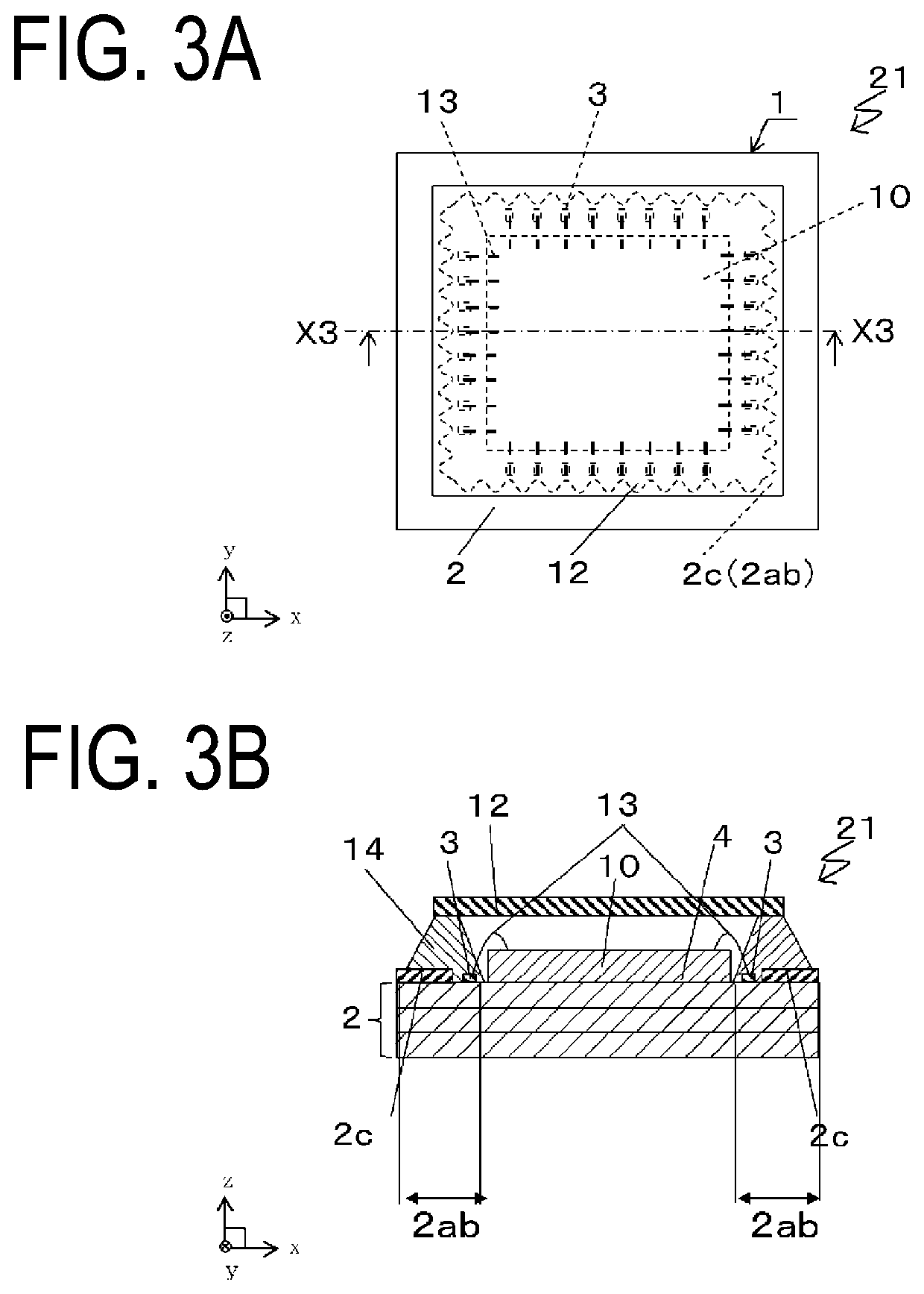
[0072]The electronic device 21, an electronic module 31, and the electronic element mounting substrate 1 according to the third embodiment of the present disclosure will be described with reference to FIGS. 4 and 5. Note that in the present embodiment, FIG. 4 illustrates the electronic device 21. FIG. 5 illustrates the electronic device 21 with a casing 32 (lens) mounted instead of the lid 12.
[0073]The electronic element mounting substrate 1 includes the substrate 2a and at least one insulating layer 2c located on an upper surface of the substrate 2a and including the mounting region 4 where the electronic element 10 is mounted on the upper surface. The insulating layer 2c includes an opening portion 5, and the plurality of electrode pads 3 are located in the opening portion 5.
[0074]In this embodiment, the structure of the electronic device 21, the substrate 2a, the electrode pads 3, the insulating layer 2c, the electronic element 10, and the like constituting the electronic element...
PUM
 Abstract
Description
Claims
Application Information
 - R&D Engineer
- R&D Manager
- IP Professional
- Industry Leading Data Capabilities
- Powerful AI technology
- Patent DNA Extraction
Browse by: Latest US Patents, China's latest patents, Technical Efficacy Thesaurus, Application Domain, Technology Topic, Popular Technical Reports.
© 2024 PatSnap. All rights reserved.Legal|Privacy policy|Modern Slavery Act Transparency Statement|Sitemap|About US| Contact US: help@patsnap.com