Sense amplifying circuit of semiconductor memory device
a memory device and sense amplifier technology, applied in the field of semiconductor memory device sense amplifiers, can solve the problems of reducing the effective sensing margin affecting the performance of the dram, and causing offset noise of the sense amplifier, so as to maximize the potential difference in bit line pairs, improve the effective sensing margin, and maximize the voltage difference
- Summary
- Abstract
- Description
- Claims
- Application Information
AI Technical Summary
Benefits of technology
Problems solved by technology
Method used
Image
Examples
first embodiment
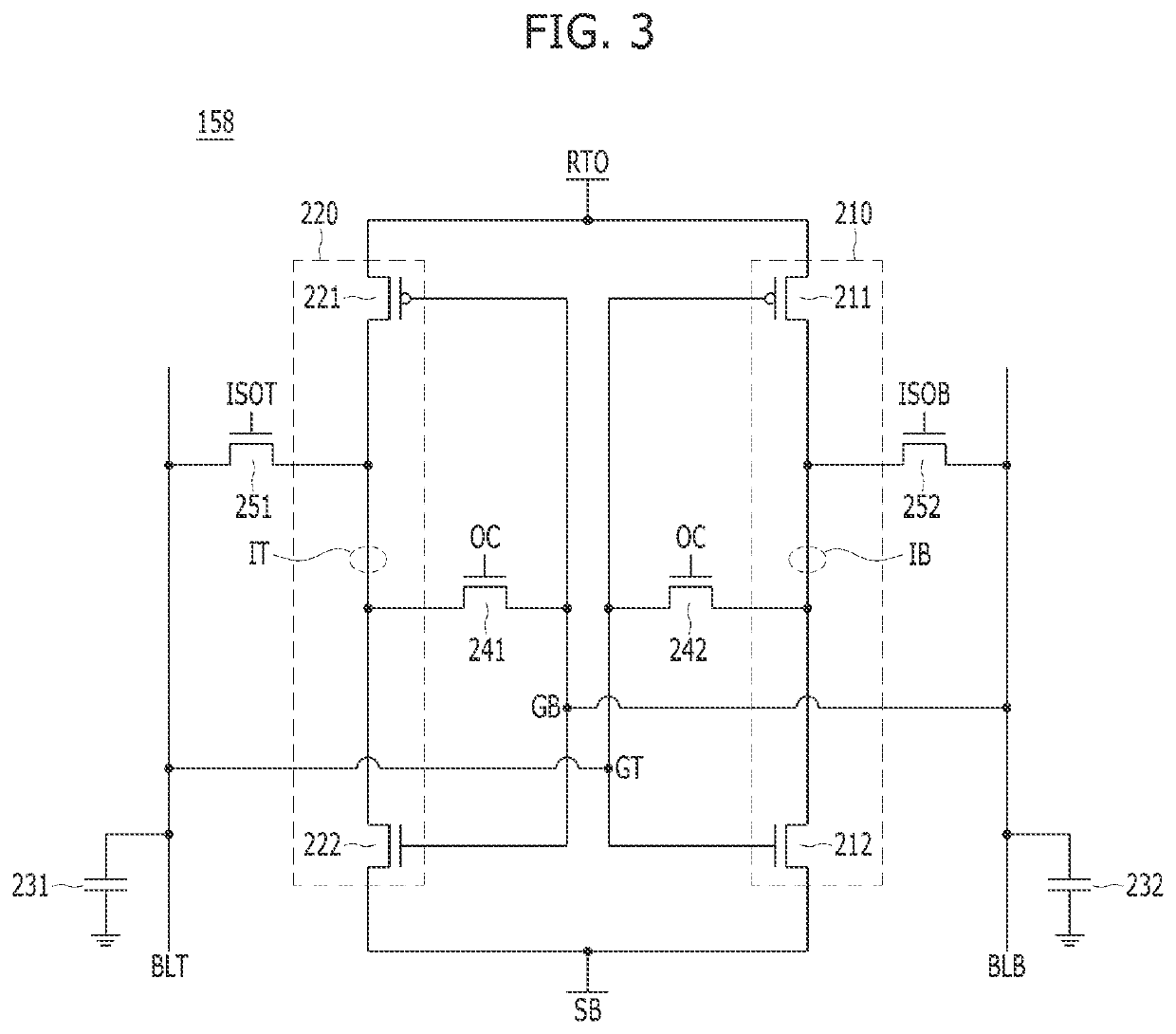
[0047]FIG. 3 is a circuit diagram illustrating a bit line sense amplifier (BLSA) 158 in accordance with the present invention.
[0048]Referring to FIG. 3, the BLSA 158 may include a first inverter 210, a second inverter 220, a first offset cancellation switch 241, a 20 second offset cancellation switch 242, a first isolation switch 251, and a second isolation switch 252.
[0049]The first inverter 210 may have an input terminal coupled to a first bit line BLT through a first sensing node GT, and an output terminal coupled to a second inner bit line IB. The first inverter 210 may include a PMOS transistor 211 and an NMOS transistor 212 coupled in series between a pull-up voltage line RTO and a pull-down voltage line SB. The second inverter 220 may have an input terminal coupled to a second bit line BLB through a second sensing node GB, and an output terminal coupled to a first inner bit line IT. The second inverter 220 may include a PMOS transistor 221 and an NMOS transistor 222 coupled i...
second embodiment
[0063]FIG. 6 is a circuit diagram illustrating a bit line sense amplifier (BLSA) 158 in accordance with the present invention.
[0064]Referring to FIG. 6, the BLSA 158 may include a pull-up circuit 310, a pull-down circuit 320, a first offset cancellation switch 341, a second offset cancellation switch 342, a first isolation switch 351, a second isolation switch 352, a first pre-biasing switch 361, and a second pre-biasing switch 362.
[0065]The pull-up circuit 310 may include a first PMOS transistor 311 and a second PMOS transistor 312. The first PMOS transistor 311 may be coupled between a pull-up voltage line RTO and a first inner bit line IT, and the second PMOS transistor 312 may be coupled between the pull-up voltage line RTO and a second inner bit line IB. Each of the first and second PMOS transistors may be disposed in a cross-coupled structure to which a drain and a gate are coupled.
[0066]The pull-down circuit 320 may include a first NMOS transistor321 and a second PMOS transis...
PUM
 Abstract
Description
Claims
Application Information
 - R&D Engineer
- R&D Manager
- IP Professional
- Industry Leading Data Capabilities
- Powerful AI technology
- Patent DNA Extraction
Browse by: Latest US Patents, China's latest patents, Technical Efficacy Thesaurus, Application Domain, Technology Topic, Popular Technical Reports.
© 2024 PatSnap. All rights reserved.Legal|Privacy policy|Modern Slavery Act Transparency Statement|Sitemap|About US| Contact US: help@patsnap.com


