Method for manufacturing a structure

a manufacturing method and structure technology, applied in the direction of semiconductor devices, semiconductor/solid-state device details, electrical devices, etc., can solve the problems of inability to achieve photolithography steps, inability to meet the requirements of photolithography, and inability to achieve treatment satisfactorily, so as to improve the wettability of the front face

Pending Publication Date: 2022-06-16
COMMISSARIAT A LENERGIE ATOMIQUE ET AUX ENERGIES ALTERNATIVES
View PDF0 Cites 0 Cited by
  • Summary
  • Abstract
  • Description
  • Claims
  • Application Information

AI Technical Summary

Benefits of technology

[0046]The second passivation layer improves the wettability of the front face and of the main face by the glue, and thus makes it

Problems solved by technology

However, this known method of the prior art is not satisfactory.
However, the step of removing the handle layer, generally executed by chemical etching or by CMP (Chemical Mechanical Polishing), leaves the meniscus M intact in such a way that the topology associated with the latter makes any step of photolithography impossible (FIG. 3).
These treatments do not however seem t

Method used


Image

  • Method for manufacturing a structure
  • Method for manufacturing a structure
  • Method for manufacturing a structure

Examples


Embodiment Construction

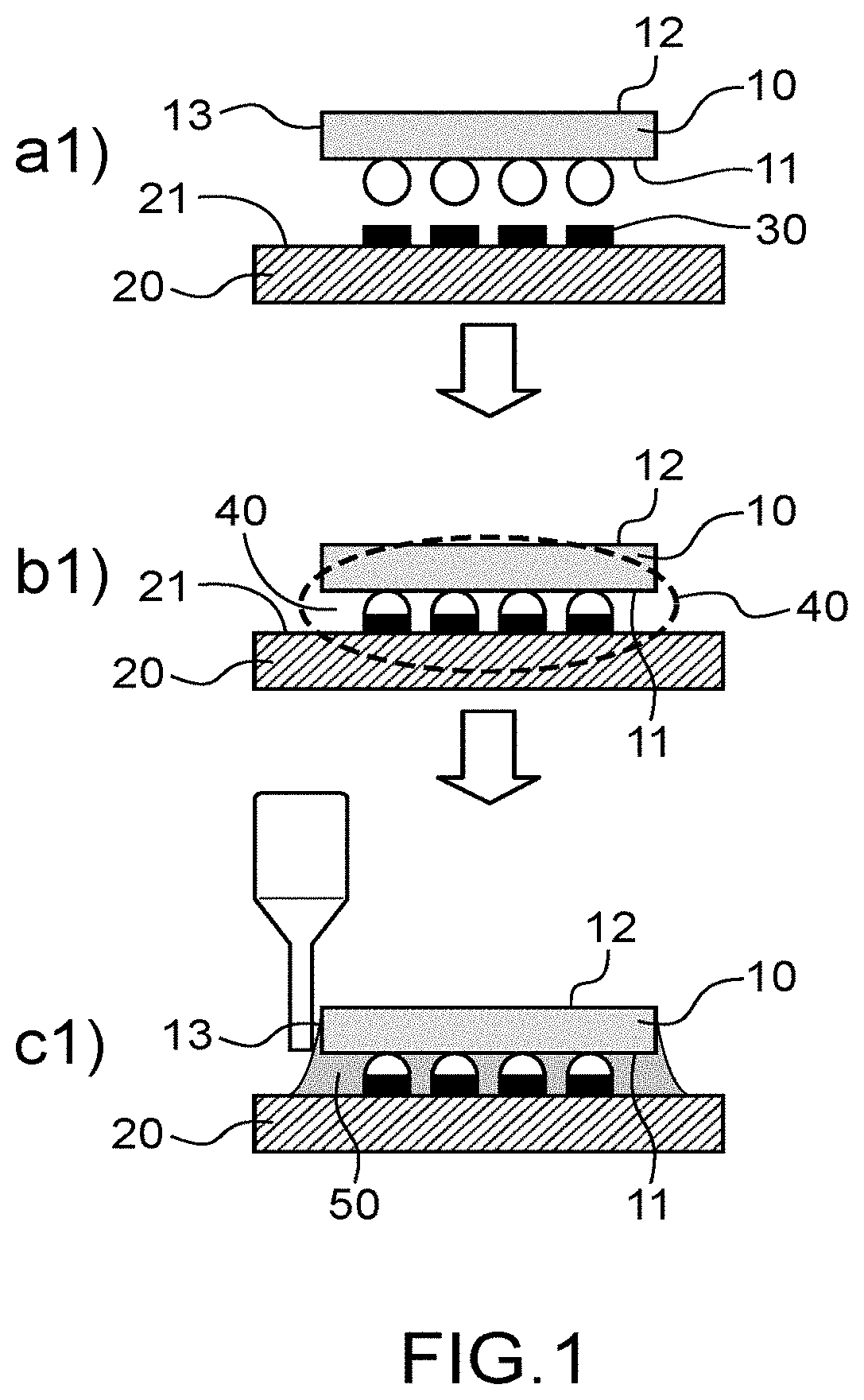
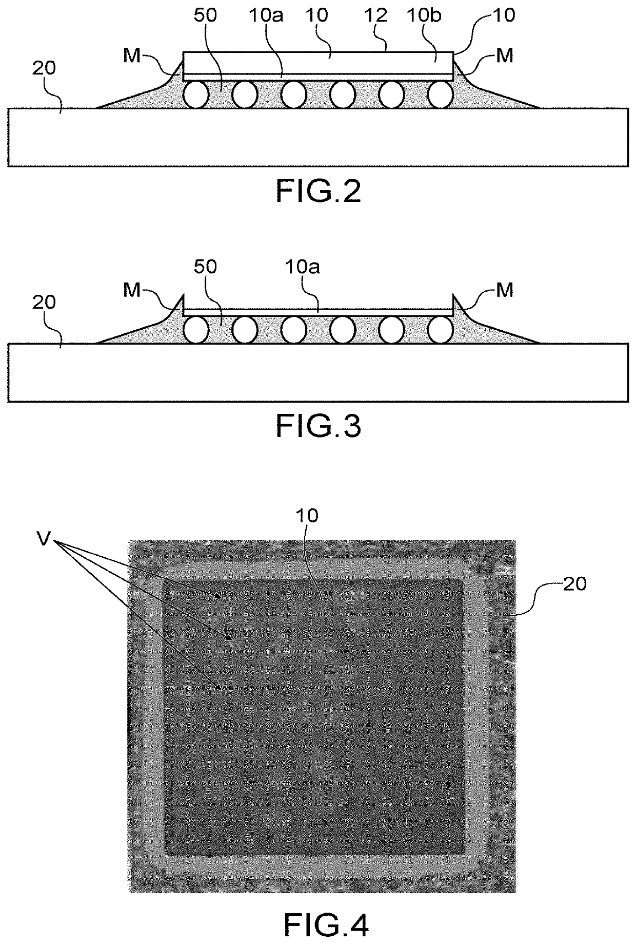
[0062]The present invention relates to a method of encapsulation by a glue of a space of interconnections that is interposed between an active element and a support to which said element is assembled.

[0063]In particular, the present invention implements a first passivation layer formed, by a method other than a plasma method, at least on a contour of the active element in such a way as to limit the wetting of said contour by the glue, and thus prevent the covering of the contour by a meniscus of glue that is formed in the vicinity of said contour.

[0064]FIGS. 5a to 5g diagrammatically show different steps of the method of manufacturing according to the present invention.

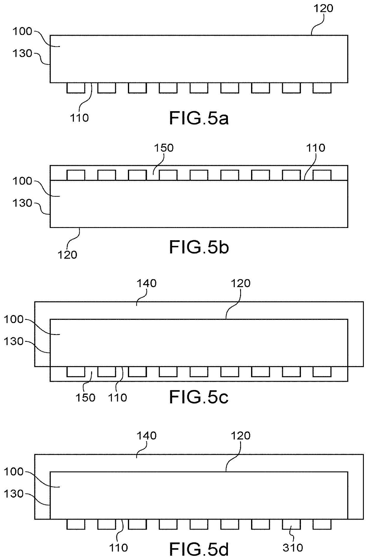
[0065]The method comprises in particular a step of supplying an active element 100 that comprises two substantially parallel faces called, respectively, front face 110 and rear face 120 (FIG. 5a).

[0066]The front face 110 and the rear face 120 are moreover connected by a contour 130.

[0067]“Contour” means a surface, wit...


PUM


Abstract

A method for manufacturing a structure includes: supplying an active element provided with a front and rear face connected by a contour; assembling the front face and a main face of a support; filling a space of interconnections between the front face and the main face with glue. The method also includes, before the assembling, forming, by a method other than a plasma method, a first passivation layer covering the contour, and made from a first compound that makes it possible to limit the wetting of said contour by the glue regarding the front face and the main face.

Description

TECHNICAL FIELD[0001]The present invention relates to a method for manufacturing a structure, and in particular a method of encapsulating a space of interconnections interposed between an active element and a support to which said element is assembled.PRIOR ART[0002]Three-dimensional integration, well known to those skilled in the art, has made many technological breakthroughs possible, in particular, for the improvement in the performance and the increase in the density of microelectronic and / or optronic devices.[0003]3D integration makes it possible in particular to decrease the interconnection lengths, and consequently the density thereof, without necessarily reducing their lateral dimensions.[0004]This technology can make use of the formation of VIAs, bumps, substrate thinning, assembly of substrates or of active elements, as well as encapsulation.[0005]In this regard, encapsulation with a glue can be implemented in order to reinforce the mechanical strength and the reliability ...

Claims


Application Information

Patent Timeline
IPC IPC(8): H01L23/00H01L21/56
CPCH01L24/83H01L2224/8385H01L24/26H01L24/32H01L2224/32221H01L24/16H01L2224/16221H01L24/73H01L2224/73204H01L24/92H01L2224/92125H01L24/13H01L2224/13166H01L2224/13144H01L2224/13083H01L2224/13147H01L2224/13155H01L2224/13111H01L2224/13139H01L2224/26145H01L2224/26175H01L24/29H01L2224/2919H01L2924/0665H01L24/81H01L2224/81815H01L2224/81193H01L2224/83007H01L21/563H01L2224/13109H01L2224/13011H01L2224/83102H01L2224/16227H01L2224/32225H01L23/3185H01L23/293H01L2924/00014H01L2924/014H01L2924/0105H01L2924/01049H01L2224/16225H01L2924/00
Inventor CAICEDO PANQUEVA, NOHORA-LIZETHAIT-MANI, ABDENACERNONGLATON, GUILLAUME
Owner COMMISSARIAT A LENERGIE ATOMIQUE ET AUX ENERGIES ALTERNATIVES
Why Eureka
Try Eureka