Stable PCB for solid state light source application

a solid-state light source and pcb technology, applied in the field of lighting devices, can solve problems such as the deformation of the dielectric layer

Pending Publication Date: 2022-07-07
SIGNIFY HLDG BV
View PDF8 Cites 0 Cited by
  • Summary
  • Abstract
  • Description
  • Claims
  • Application Information

AI Technical Summary

Problems solved by technology

By the high intensity light both solder resist layer but most importantly the dielectric layer may degrade.

Method used


Image

  • Stable PCB for solid state light source application
  • Stable PCB for solid state light source application
  • Stable PCB for solid state light source application

Examples


Embodiment Construction

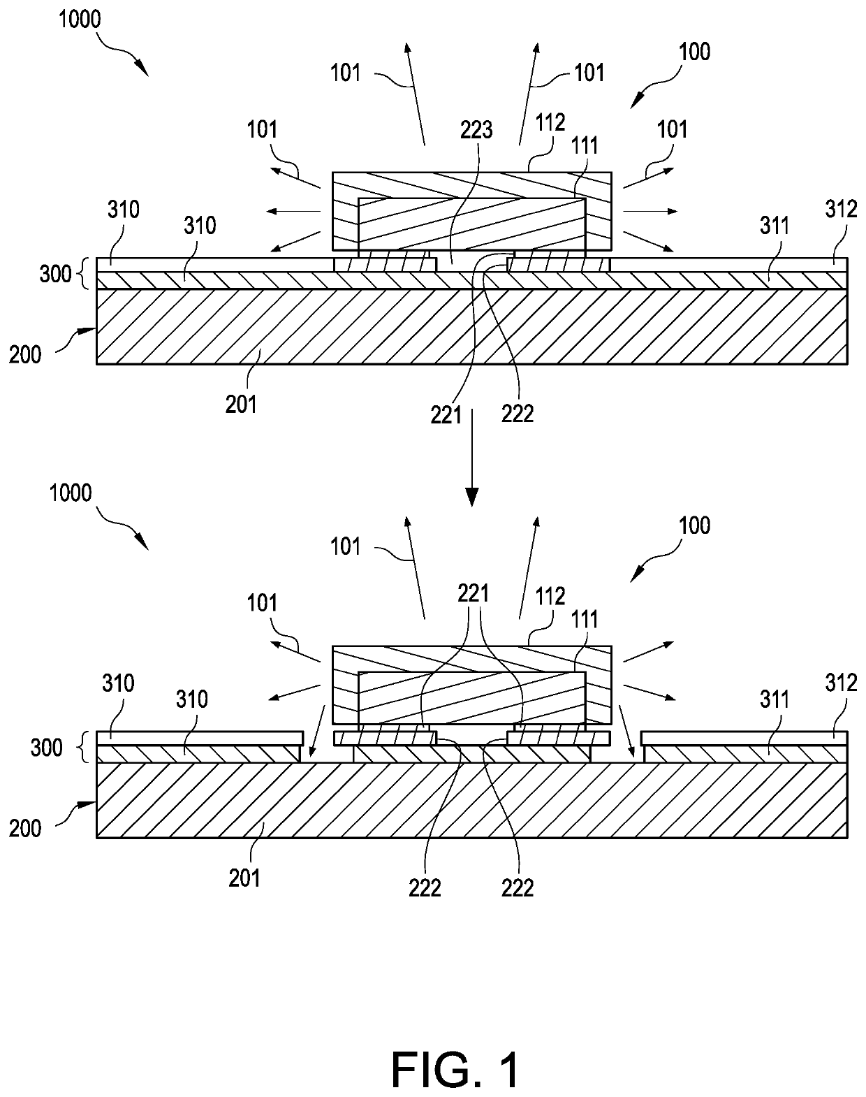
[0081]FIG. 1 schematically depicts the impact which light source light may have on a layer adjacent to the light source. Here below, FIG. 1 is described in relation to a Chip scale packaged (CSP) LED. However, the invention is not limited to CSP light sources.

[0082]Chip scale packaged (CSP) LEDs are being increasingly used in various applications because of its robust structure and attractive pricing. As opposed to the packaged LEDs, a CSP LED is placed directly on top of the printed circuit board (PCB). In the case of packaged LEDs the presence of the package stops blue light reaching the PCB. In the case CSP high intensity light from the CSP reaches the surface of the PCB. PCBs with high thermal conductivity have a metal (aluminum) base with an epoxy dielectric layer on top it below the copper tracks. Reflective solder resist layer containing reflective particles are present on the surface of the PCB except for the areas reserved for soldering the LEDs. During the operation of the...


PUM

PropertyMeasurementUnit
heightaaaaaaaaaa
heightaaaaaaaaaa
widthaaaaaaaaaa

Abstract

The invention provides a lighting device (1000) comprising (i) a light source (100) configured to generate light source light (101), wherein the light source (100) comprises a solid state light source, and (ii) a support (200) configured to support the light source (100), wherein the support (200) comprises a metal based thermally conductive material (201), wherein the lighting device (1000) further comprises (iii) a layered element (300), configured in physical contact with the support (200), wherein the layered element (300) comprises one or more layers (310), wherein the layered element (300) at least comprises an electrically insulating first layer (311), wherein at least part of the layered element (300) is configured between the light source (100) and the support (200) such that during operation part of the light source light (101) irradiates the layered element (300), wherein the layered element (300) comprises light reflective particles (410), wherein at least 50 wt. % of the particles have a flake-like shape.

Description

FIELD OF THE INVENTION[0001]The invention relates to a lighting device comprising (i) a light source configured to generate light source light and (ii) a support configured to support the light source. The invention also provides a lamp or luminaire, comprising such lighting device.BACKGROUND OF THE INVENTION[0002]An insulation film coated and formed as a protective film in a printed-wiring board is known in the art. US2009 / 0141505 indicates in relation to such film that in addition to characteristics such as solvent resistance, hardness, solder resistance and electrical insulating properties generally required in a solder resist film, an excellent light reflectivity capable of utilizing emission of LED effectively has been desired. US2009 / 0141505 describes e.g. a white heat-hardening resin composition comprising rutile-type titanium oxide; and a heat-hardening resin.SUMMARY OF THE INVENTION[0003]Chip scale packaged (CSP) LEDs are being increasingly used in various applications beca...

Claims


Application Information

Patent Timeline
Patent Type & Authority Applications(United States)
IPC IPC(8): H05K1/02F21V19/00F21V29/503
CPCH05K1/0274F21V19/0025F21Y2115/10H05K1/0203F21V29/503H05K1/056H05K2201/0245H05K2201/10106H05K2201/2054H05K2201/0224
Inventor HIKMET, RIFAT ATA MUSTAFAVAN BOMMEL, TIESONUSHKIN, GRIGORY
Owner SIGNIFY HLDG BV
Why Eureka
Try Eureka