Organic electroluminescent device

Pending Publication Date: 2022-07-14
WUHAN CHINA STAR OPTOELECTRONICS SEMICON DISPLAY TECH CO LTD
View PDF0 Cites 0 Cited by
  • Summary
  • Abstract
  • Description
  • Claims
  • Application Information

AI Technical Summary

Problems solved by technology

When electrons and holes in TEOLEDs have great different transmission capabilities, carriers, including electrons and holes, are injected at greatly different rates, so that an exciton recombination region of the device deviates from the light emitting layer and is close to a side of carriers having a lower transmission capability, and the recombination region is narrow, which is disadvantageous to the continuous improvement of devices lifetime and efficiency.
Studies have shown that cathode deposited in the vapor deposition proce

Method used


Image

  • Organic electroluminescent device
  • Organic electroluminescent device
  • Organic electroluminescent device

Examples


Example

[0035]The specific structural and functional details disclosed herein are merely representative and are for purposes of describing exemplary embodiments of the present invention. The present invention, however, may be implemented in many alternative ways and should not be construed as being limited to the embodiments set forth herein.

[0036]In the description of the present invention, it should be understood that the terms including “center,”“lateral,”“upper,”“lower,”“left,”“right,”“vertical,”“horizontal,”“top,”“bottom,”“inside,” and “outside” are based on the orientation or positional relationship shown in the drawings, and the terms are merely for convenience of description of the present invention and simplified description, and do not indicate or imply the indicated device or the components must have a specific orientation, specific orientation structure, and operation, and thus they are not to be construed as limiting. Moreover, the terms “first” and “second” are only used for d...


PUM


Abstract

An organic electroluminescent device includes an anode, a cathode disposed opposite to the anode, and a light emitting functional layer disposed between the anode and the cathode. The light emitting functional layer includes a light emitting layer and a PN junction layer disposed on a side of the light emitting layer, and when a positive charge is applied to the anode and a negative charge is applied to the cathode, the PN junction layer forms an open circuit, so that the cathode and the anode evenly inject carriers into the light emitting layer.

Description

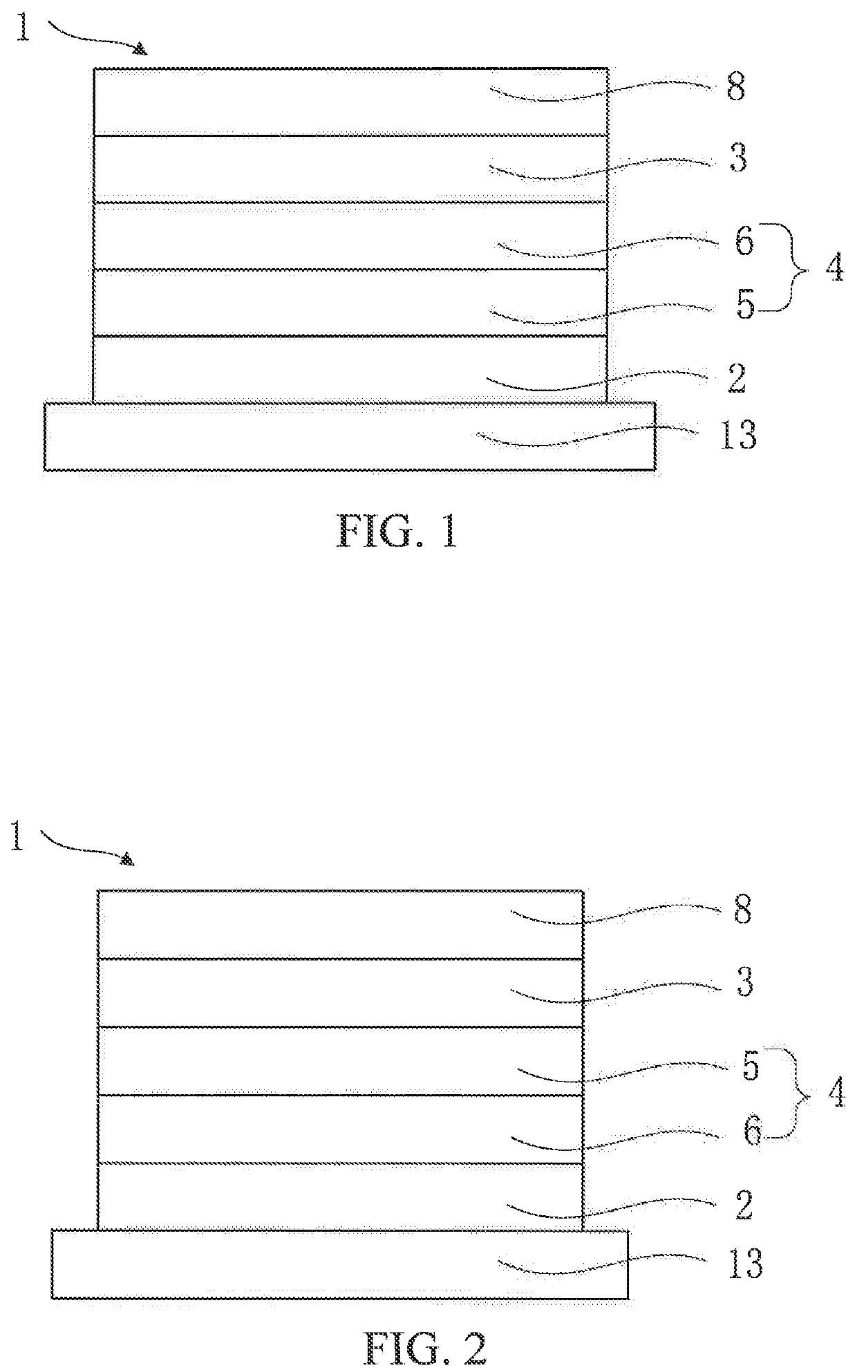
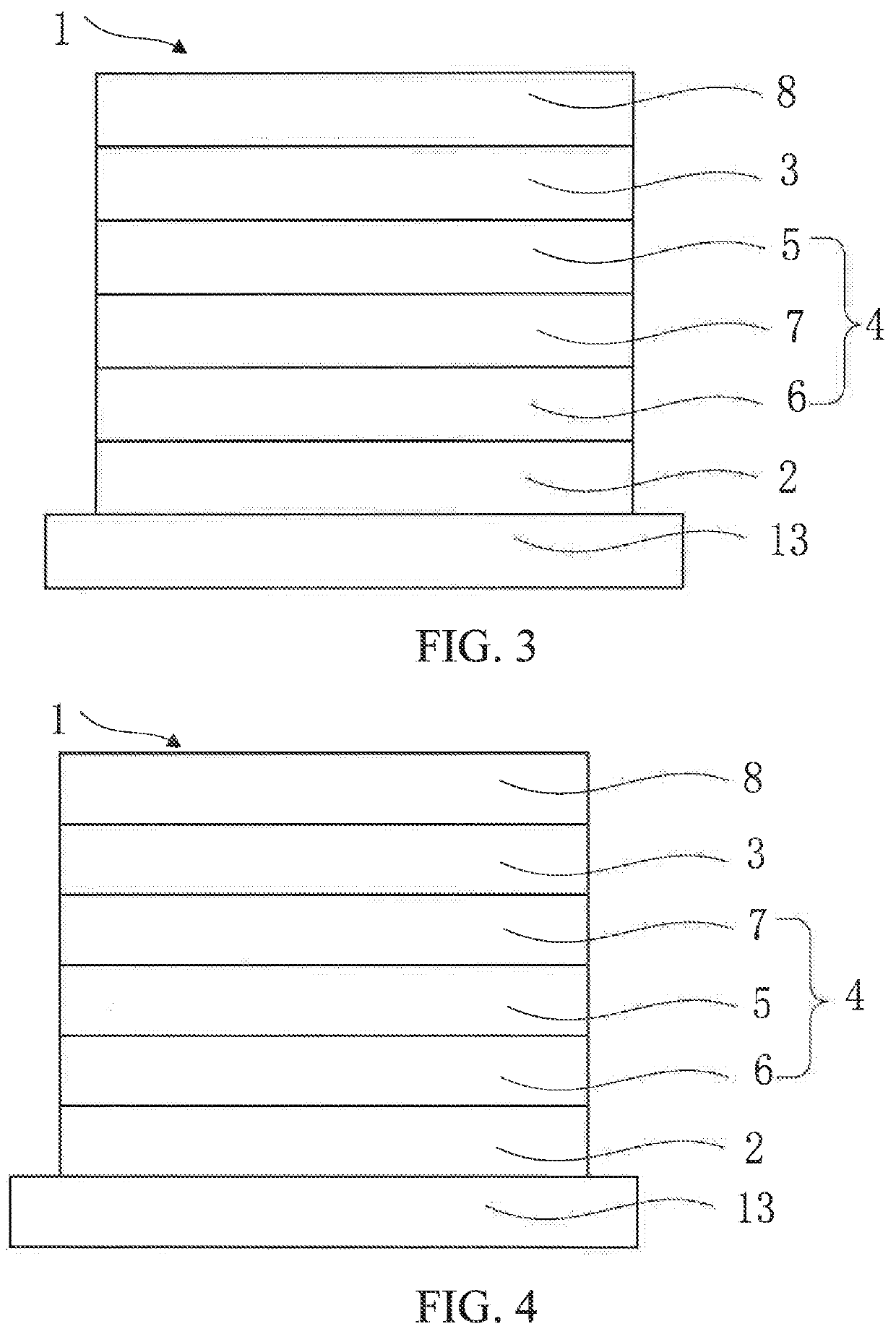
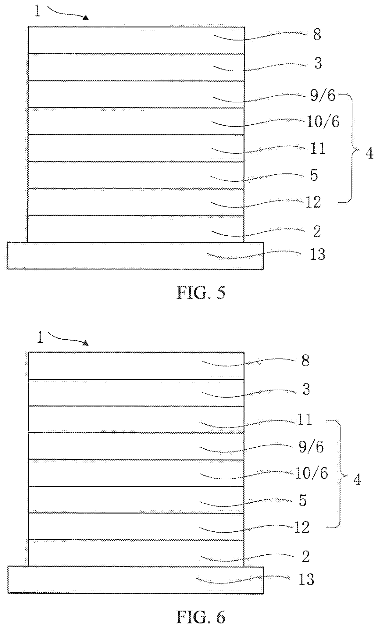
FIELD OF INVENTION[0001]The present invention relates to a field of display panel, and more particularly, to an organic electroluminescent device.DESCRIPTION OF PRIOR ART[0002]The statements herein merely provide background information related to the present application and do not necessarily constitute prior art.[0003]Organic light emitting diode (OLED) devices have self-illumination, ultra-thin, low power consumption, and high contrast, and they can be applied to flexible displays. Thus, OLED devices have been focused and studied in the display industry.[0004]Most of the OLED devices used in flat panel displays are top-emitting OLEDs (TEOLEDs). When electrons and holes in TEOLEDs have great different transmission capabilities, carriers, including electrons and holes, are injected at greatly different rates, so that an exciton recombination region of the device deviates from the light emitting layer and is close to a side of carriers having a lower transmission capability, and the ...

Claims


Application Information

Patent Timeline
IPC IPC(8): H01L51/50
CPCH01L51/5076H01L51/506H01L51/5012H01L51/5092H01L51/5096H10K50/11H10K50/18H10K50/16H10K50/156H10K50/155H10K50/166H10K50/165H10K50/171
Inventor DING, KE
Owner WUHAN CHINA STAR OPTOELECTRONICS SEMICON DISPLAY TECH CO LTD
Why Eureka
Try Eureka