Deposition of alpha-gallium oxide thin films

Pending Publication Date: 2022-07-21
RAFIE BORUJENY ELHAM
View PDF3 Cites 0 Cited by
  • Summary
  • Abstract
  • Description
  • Claims
  • Application Information

AI Technical Summary

Benefits of technology

The present invention is about a way to grow high-quality α-Ga2O3 on GaN-compatible substrates with control over the crystal structure. This is done using a special deposition approach that involves plasma-enhanced ALD. This approach minimizes the formation of unwanted byproducts and allows for the integration of GaN and Ga2O3 components on a single substrate. This invention helps to fast-track the development of Ga2O3 electronics and take advantage of advancements in GaN technology.

Problems solved by technology

However, there are currently a number of challenges that limit the development of β-Ga2O3 electronic devices including inherent complexities in its crystal structure, limited success in heteroepitaxial growth of β-Ga2O3 on foreign substrates (see below Reference no.

Method used


Image

  • Deposition of alpha-gallium oxide thin films
  • Deposition of alpha-gallium oxide thin films
  • Deposition of alpha-gallium oxide thin films

Examples


experimental example

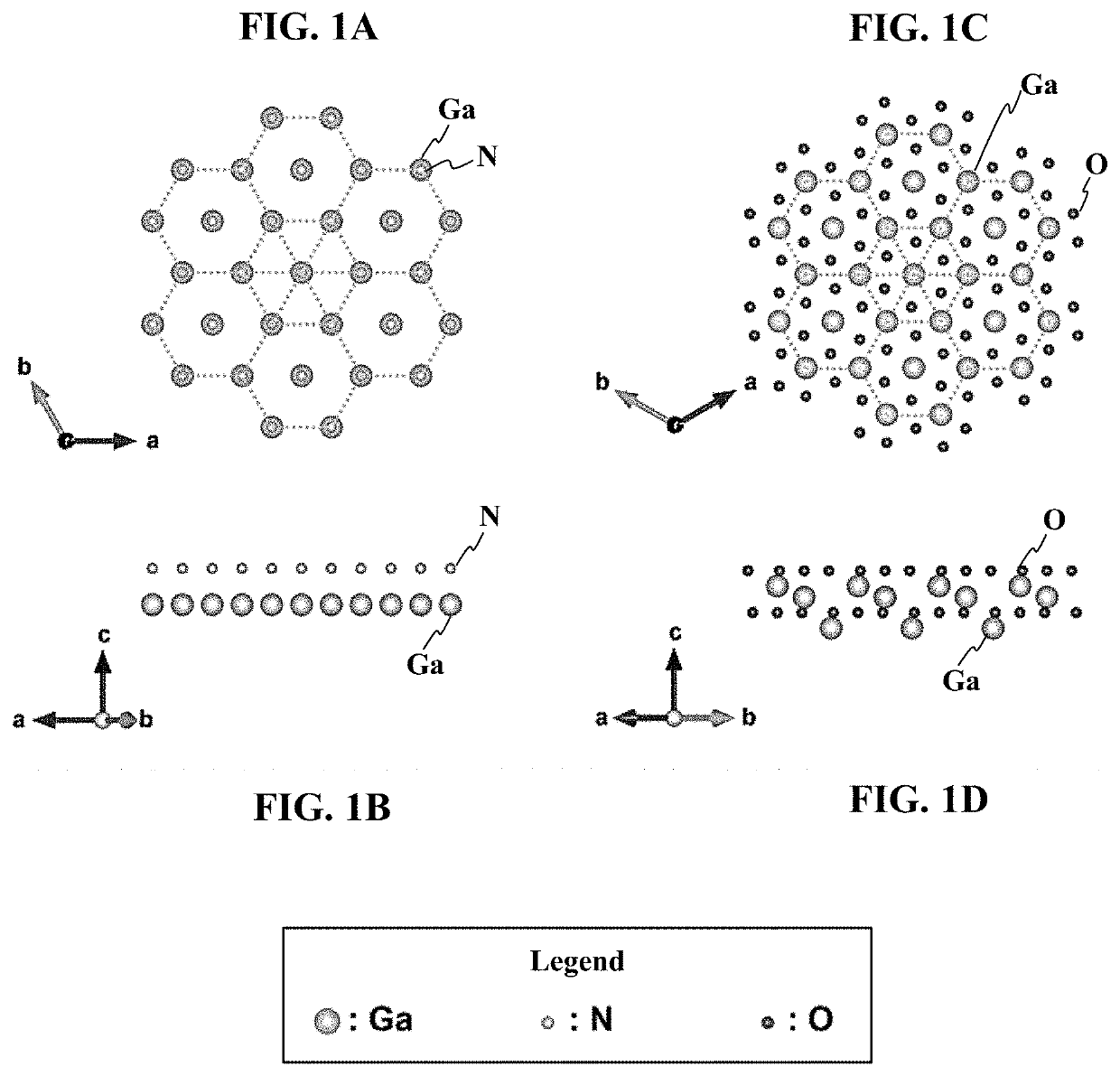
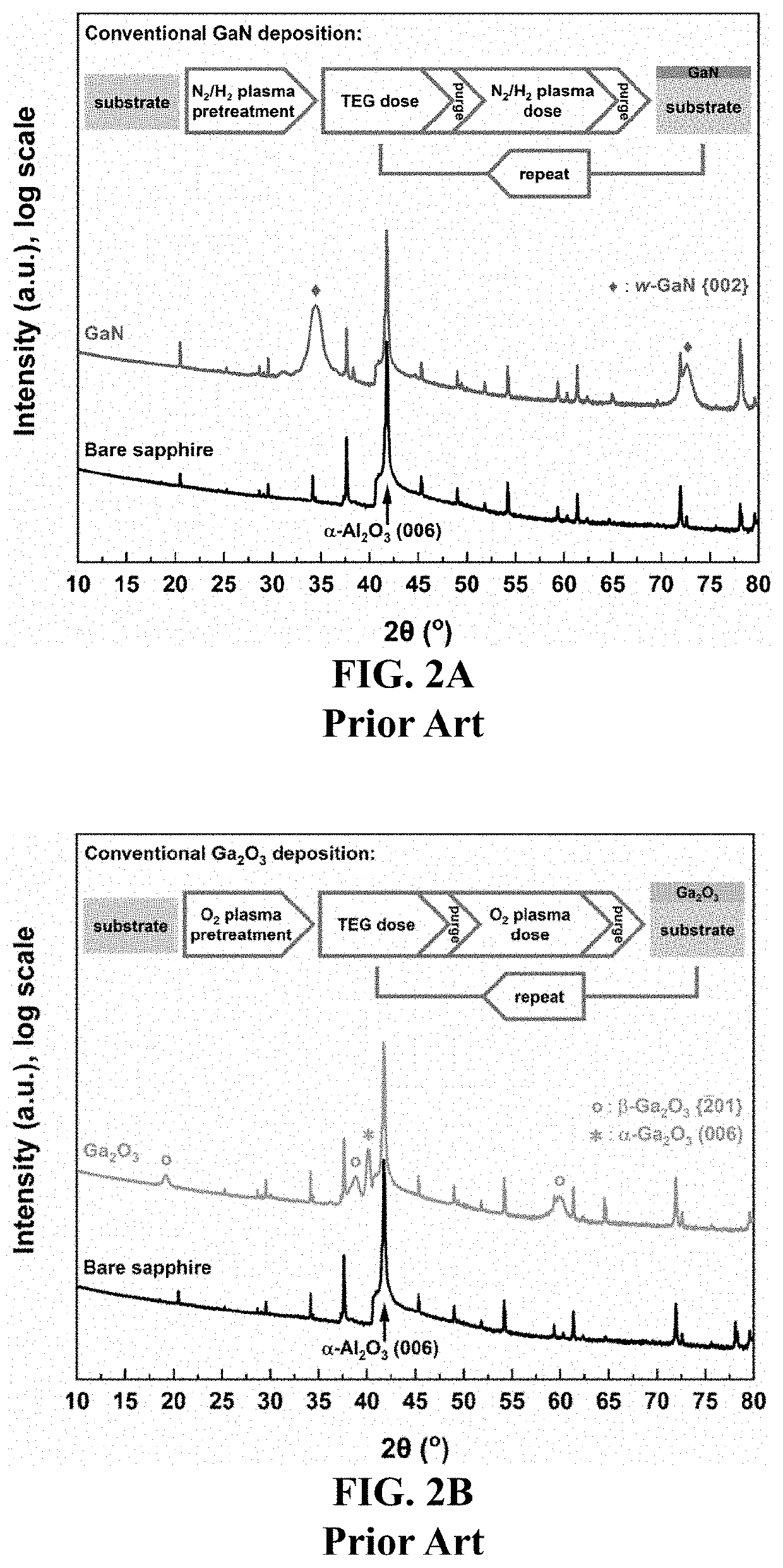
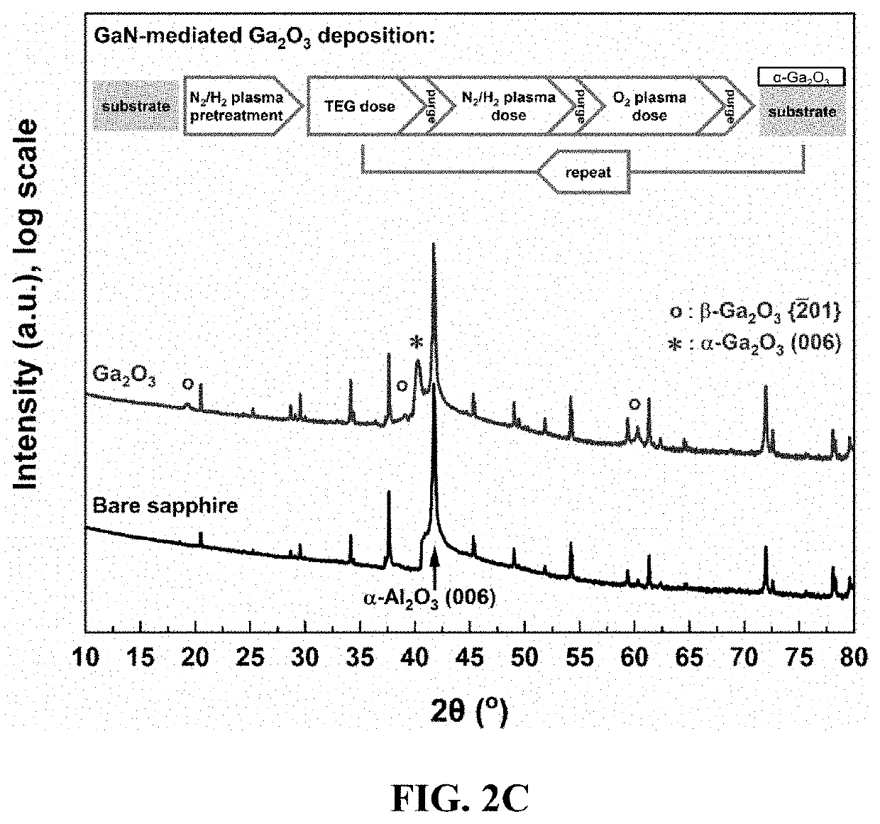
[0075]Depositions were done at 277° C. on single-side polished (Ra2 / H2 forming gas was introduced to the reactor during plasma exposures with ˜600 W forward power. This setup is also explained in detail elsewhere (see below References no. 6 and 23). Triethylgallium, TEG, (Strem Chemicals, Inc.) was electronic grade (99.9999% Ga) in a stainless steel Swagelok™ cylinder assembly which was not heated during the depositions; all other gases (argon, oxygen, and forming gas) were of ultrahigh purity (99.999%, Praxair Canada, Inc.). Substrates were exposed to 60 s plasma to remove contamination and pretreat the surface prior to deposition. Reference GaN depositions were done by using a recipe consisting of 0.1 s TEG dose, 3 s argon purge, 15 s N2 / H2 forming gas plasma dose, and 2 s argon purge. Reference Ga2O3 depositions were done by using a recipe consisting of 0.1 s TEG dose, 20 s argon purge, 10 s oxygen plasma dose, and 12 s argon purge (reducing the two purge times down to 3 s and 2 ...


PUM

PropertyMeasurementUnit
Temperatureaaaaaaaaaa
Fractionaaaaaaaaaa
Timeaaaaaaaaaa

Abstract

A method for forming alpha-gallium oxide (α-Ga2O3) on GaN-compatible substrates uses an epitaxial deposition process comprising (a) forming about one monolayer of wurtzite gallium nitride (w-GaN) on the substrate; (b) reacting the said monolayer of w-GaN with an oxygen precursor to form about one monolayer of α-Ga2O3 on the substrate; (c) repeating steps (a) and (b) to form one or more additional monolayers of α-Ga2O3 on the substrate.

Description

CROSS-REFERENCE TO RELATED APPLICATION[0001]This application claims priority to U.S. Provisional Patent Application No. 63 / 137,874, filed on Jan. 15, 2021, the entire disclosure of which is incorporated by reference herein in its entirety for all purposes.FIELD OF THE INVENTION[0002]The present invention relates to forming semiconductor thin films, using epitaxial deposition processes.BACKGROUND OF THE INVENTION[0003]Research into new materials for power electronic devices has emerged as an inseparable part of sustainable development and efficient handling of electrical energy during the past three decades. Such power devices may convert DC power generated by solar cells and fuel cells to AC power, thereby making it usable by consumers. Alternatively, such power devices may convert AC power supplied by a provider to DC power, thereby making it usable in charging the battery of an electric car or a portable electronic device.[0004]Wide bandgap semiconductors such as GaN (gallium nitr...

Claims


Application Information

Patent Timeline
IPC IPC(8): C30B25/18H01L21/02C23C16/40C23C16/455C30B29/16
CPCC30B25/18H01L21/0242H01L21/02458H01L21/02513H01L21/02565C30B29/16H01L21/0262C23C16/40C23C16/45553C23C16/45536H01L21/02598H01L21/02612H01L21/02609C23C16/45542
Inventor RAFIE BORUJENY, ELHAM
Owner RAFIE BORUJENY ELHAM
Why Eureka
Try Eureka