Eureka AIR delivers breakthrough ideas for toughest innovation challenges, trusted by R&D personnel around the world.

Packaged electronic system formed by electrically connected and galvanically isolated dice

Pending Publication Date: 2022-07-28
STMICROELECTRONICS SRL
View PDF0 Cites 0 Cited by
  • Summary
  • Abstract
  • Description
  • Claims
  • Application Information

AI Technical Summary

Benefits of technology

The present disclosure provides a solution to overcome the drawbacks of conventional packaging structures. A packaged electronic system is provided that includes a support with a buried conductive region and a connection pad, as well as two die (a first and a second) with capacitively coupled contact regions that are connected to external connection regions through a connection line. The system is enclosed in a packaging mass. The technical effect is to provide a more efficient and cost-effective packaged electronic system with improved signal integrity and reduced interference between the components.

Problems solved by technology

In particular, with this approach, the designer is not always able to use the most advanced approaches and knowledge and frequently cannot use the same isolation elements when the circuits 10 of the dice 8, 9 are manufactured using different technologies.
However, this approach has parasitic components due to the first connection wires 35 and, in particular, the second connection wires 36, which can cause problems of cross-talk, i.e., interference between the signal-transmission channels.
However, not even these approaches are altogether satisfactory and / or can be applied to all systems.
In fact, the provision of shielding coatings cannot be used for wires of small dimensions and is subject to problems of repeatability, so that it is far from effective.
The use of high capacitances is not moreover always possible since they cause an increase in power consumption of the system and can reduce the bandwidth usable for the communications.

Method used


Image

  • Packaged electronic system formed by electrically connected and galvanically isolated dice
  • Packaged electronic system formed by electrically connected and galvanically isolated dice
  • Packaged electronic system formed by electrically connected and galvanically isolated dice

Examples


Embodiment Construction

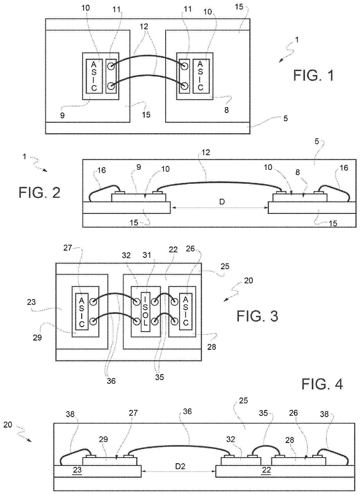
[0032]In the following description, reference will be made to a system formed by two dice, integrating each an ASIC (Application-Specific Integrated Circuit), but the disclosure applies to electronic devices of any type, whether single components or more complex circuits, operating at different voltages, even having a very different value, in common mode.

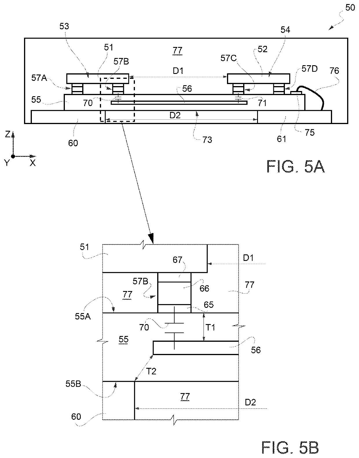
[0033]FIG. 5A shows a system 50 comprising two dice 51, 52 integrating each an own device 53, 54. The devices 53, 54 are here both ASICs, as indicated above. The two dice are spaced apart from each other by a distance D1 as shown in FIG. 5A. The distance D1 extends between respective sidewalls of the first die 51 and the second die 52.

[0034]The dice 51, 52 are both fixed to a support 55. The support 55 has, for example, a parallelepipedal shape having a first and a second main face 55A, 55B (see also the detail of FIG. 5B). The first and second main faces 55A, 55B may be referred to as surfaces (e.g., a first surface, a second surfa...


PUM


Abstract

A packaged electronic system having a support formed by an insulating organic substrate housing a buried conductive region that is floating. A first die is fixed to the support and carries, on a first main surface, a first die contact region capacitively coupled to a first portion of the buried conductive region. A second die is fixed to the support and carries, on a first main surface, a second die contact region capacitively coupled to a second portion of the buried conductive region. A packaging mass encloses the first die, the second die, the first die contact region, the second die contact region, and, at least partially, the support.

Description

BACKGROUNDTechnical Field[0001]The present disclosure relates to a packaged electronic system formed by electrically connected and galvanically isolated dice.Description of the Related Art[0002]Electronic systems where the dice are packaged in a package and integrate electronic devices (components and / or circuits) configured to work at very different voltages and to exchange signals with each other. For instance, the electronic systems may be a power-supply system, a digital isolator, a power transistor driving system, a DC-DC converter, or other system where at least one of the devices operates at high voltage (even higher than 10 kV) and / or high power. For these systems, it is known to include measures for maintaining an adequate isolation galvanic between the various devices.[0003]In particular, packages dedicated to providing a high isolation level are mainly based upon two approaches:[0004]two-dice approach, where two dice integrate each a respective “functional” device and a r...

Claims


Application Information

Patent Timeline
IPC IPC(8): H01L25/065H01L23/64H01L23/00H01L23/538
CPCH01L25/0652H01L23/642H01L23/5384H01L23/5386H01L24/14H01L23/49838H01L25/0655H01L23/3107H01L23/5383H01L23/49816H01L23/48H01L2224/16227H01L23/49558H01L2924/19107H01L2224/0401H01L2224/16265H01L2924/19104H01L2924/19041H01L2224/16235H01L2924/15311H01L2224/73253H01L2224/32245H01L24/16H01L23/49575H01L23/49531H01L23/4951
Inventor PACI, DARIOADORNO, SILVIADEL SARTO, MARCOCERINI, FABRIZIOGRITTI, ALEX
Owner STMICROELECTRONICS SRL
Why Eureka
Eureka Blog
Learn More