

Afferent neuron circuit and mechanoreceptive system
a mechanoreceptive system and neuron circuit technology, applied in biological neural network models, instruments, semiconductor devices, etc., can solve the problems of poor scalability, complex structure, and inapplicability to large-scale integration use, and achieve the effect of simple structur
- Summary
- Abstract
- Description
- Claims
- Application Information
AI Technical Summary
Benefits of technology
Problems solved by technology
Method used
Image

Examples
embodiment 1
of the Present Disclosure
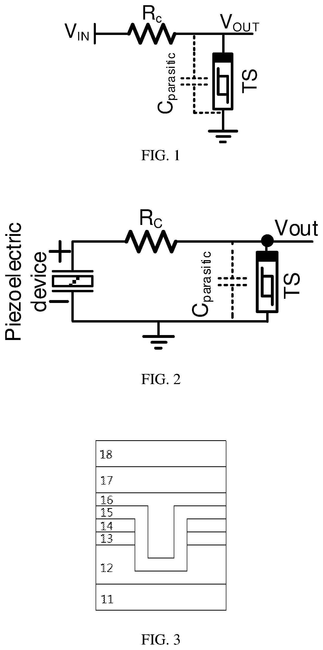
[0033]Referring to FIG. 1, the present embodiment provides an afferent neuron circuit, including a resistance Rc and a volatile threshold switching device TS. The volatile threshold switching device TS is provided with a parasitic capacitor Cparasitic. A first end of the resistance Rc serves as a signal input terminal, and a second end of the resistance Rc serves as a signal output terminal. A first end of the volatile threshold switching device TS is connected to the signal output terminal, and a second end of the volatile threshold switching device TS is grounded.
[0034]An input signal is a voltage signal or a current signal, and an output signal is an oscillation frequency signal. An oscillation frequency of the output signal is related to the strength of the input signal.
[0035]When there is an input signal at the signal input terminal, the parasitic capacitor Cparasitic is charged by the circuit through the resistance Rc.
[0036]In the case that a voltage a...
embodiment 2
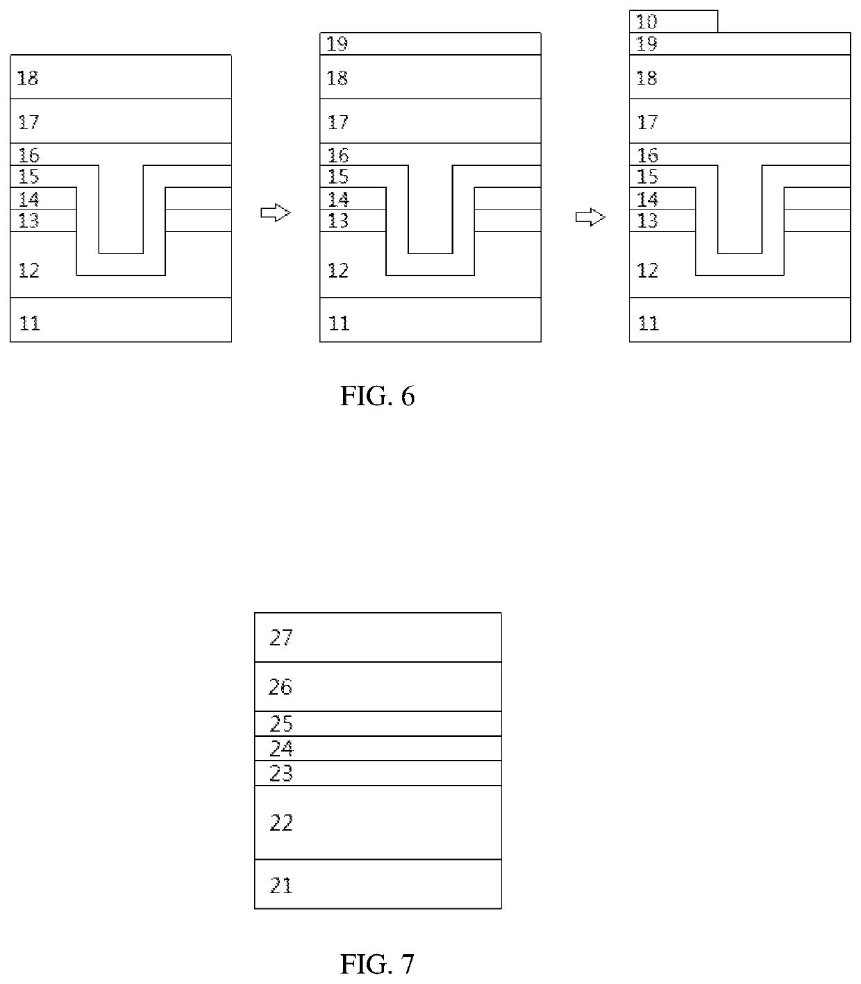
[0073]Referring to FIG. 7, on the basis of the Embodiment 1, another implementation of a volatile threshold switching device TS is provided.
[0074]The volatile threshold switching device TS includes:[0075]a second substrate 21;[0076]a third isolation layer 22, which is formed on the second substrate 21;[0077]a second lower electrode 23, which is formed on the third isolation layer 22;[0078]a second functional layer 24, which is formed on the third isolation layer 23; and[0079]a second intermediate electrode 25, which is formed on the second functional layer 24;[0080]wherein a second resistive film 26 is deposited on the second intermediate electrode 25 to serve as the resistance Rc; and a second upper electrode 27 is deposited on the second resistive film 26.
[0081]In the present embodiment, the second substrate 21 is a silicon wafer;[0082]the third isolation layer 22 is a SiO2 layer;[0083]the material of the second lower electrode 23 is an inert conductive material, such as TiN, Poly...
PUM
 Abstract
Description
Claims
Application Information