Image forming apparatus

a technology of forming apparatus and forming tube, which is applied in the direction of instruments, discharge tubes, tubes with screens, etc., can solve the problems of damage to the electron emitting device, serious damage thereby caused, and the same damage is caused

Inactive Publication Date: 2000-01-04
CANON KK
View PDF9 Cites 22 Cited by
  • Summary
  • Abstract
  • Description
  • Claims
  • Application Information

AI Technical Summary

Benefits of technology

Another object of the present invention is to provide an image forming apparatus capable of forming a full-color image with reduced color unevenness and improved color reproducibility.
Still another object of the present invention is to provide an image forming apparatus which does not require strict positioning of the image forming members and the electron emitting sections of the electron emitting devices, and which can easily be manufactured.

Problems solved by technology

In the above-described conventional image forming apparatus, however, the image forming members (luminescent members) are disposed in the space above the electron emitting devices (in the electron emitting direction) so as to face the electron emitting devices, and the following problems are therefore encountered.
Consequently, these positive ions collide against and damage the electron emitting devices.
The extent of damage thereby caused is seriously large if the device is driven under a condition that the degree of vacuum inside the device is not higher than a level at 10.sup.-5 torr.
Even if high vacuum is maintained in the device, the same damage is caused during a long-time continuous operation of the device.
Such damage to the electron emitting device results in a reduction in the electron emission rate (electron emission efficiency) and, in the worst case, breakdown of the device.
2 It is difficult to strictly align the positions of the image forming members (luminescent members) and the electron emitting sections of the electron emitting devices in a horizontal direction, and a small deviation of the position results in a considerable reduction in the contrast of the formed image (luminance unevenness or a luminance fluctuation of the luminescent image).
3 It is difficult to maintain a certain distance between the image forming members (luminescent members) and the electron emitting sections of the electron emitting devices, and a change in this distance (due to an impact or a thermal deformation during driving) results in an unintended reduction in the contrast of the formed image (luminance unevenness or a luminance fluctuation of the luminescent image).
4 Further, by the phenomena of the problems 2 and 3, color unevenness is caused in the case of an image forming apparatus having image forming members formed of multicolor luminescent materials having colors red, green and blue, resulting in a deterioration in color reproducibility according to an information signal.
Also, there is a possibility of a change in the quality of image forming members and, therefore, hot cathodes and image forming members cannot be arranged at a high density.
Ions thereby caused collide against the electron emitting element 2 and damage the same so that the electron emission rate (electron emission efficiency) is seriously reduced, resulting in a reduction in the life of the device.
Such a negative potential surface may cause a reduction in the efficiency at which the image forming member is irradiated with the electron beam or the electron beam modulation efficiency.

Method used


Image

  • Image forming apparatus
  • Image forming apparatus
  • Image forming apparatus

Examples


embodiment 35

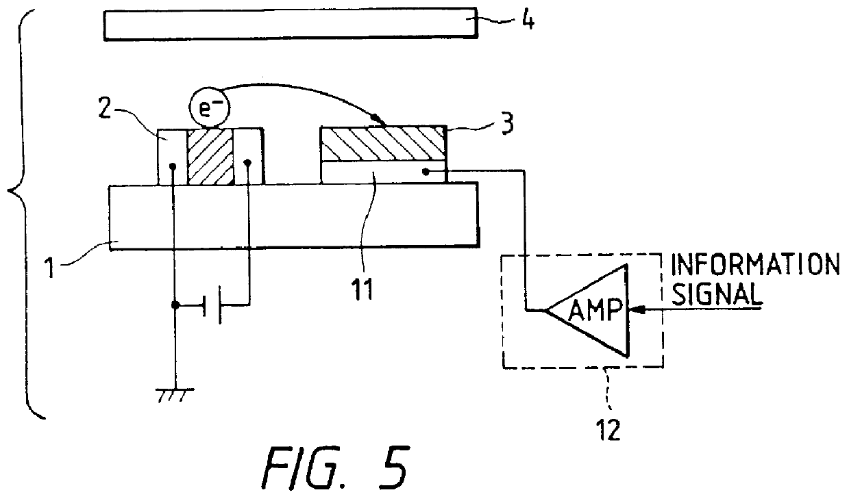
FIG. 55 is a perspective view of an image forming apparatus in accordance with a thirty-fifth embodiment of the present invention, FIG. 56 is an enlarged sectional view of a portion of the apparatus shown in FIG. 55, and FIG. 57 is a plan view of the portion shown in FIG. 56, and FIG. 58 is a cross-sectional view taken along the line A-A' of FIG. 56. As shown in these figures, this apparatus includes electron emitting devices 510 which have pairs of plus and minus electrodes 514a and 514b and each of which emits electrons when a voltage is applied between the corresponding pair of electrodes, and image forming members 516 which form an image when irradiated with beams of electrons emitted from the electron emitting devices 510. These devices and members are provided on an insulating substrate 512. The creeping distance from each image forming member 516 to the electron emitting device 510 located on the substrate 512 closest to the the image forming member 516, or to device wiring e...

embodiment 36

An apparatus in accordance with this embodiment has the same construction as Embodiment 35 and is manufactured in the same manner except that both the pitch of the arrangement of each pair of device wiring electrodes 513a and 513b and the pitch of the arrangement of electron emitting sections 515 along the device wiring electrodes are set to 1 mm. However, the voltage applied to image forming members 516 during driving is 20 to 800 V.

This embodiment achieves the same effect as Embodiment 35 while reducing the pixel pitch, that is, an image forming apparatus further improved in resolution can be obtained.

embodiment 37

This embodiment is constructed based on Embodiment 35 in such a manner that ITO electrodes in the form of strips are provided on a surface of a face plate 519 in positions such as to face image forming members 516 and image forming member wiring electrodes 520. While a constant voltage is applied to the image forming member wiring electrodes 520, voltages in accordance with an information signal are applied to the ITO electrodes to control the operation of turning on / off the emission of electron beams. A voltage of 2 kV is applied to the image forming members 516. In this case, a modulation through the ITO electrode is more preferable than a modulation with a voltage applied to the image forming member 516. This embodiment achieves a further improvement in the luminance of the displayed image.


PUM


Abstract

An image forming apparatus having a plurality of electron emitting devices and luminescent members are arranged into a matrix formed on one surface of a substrate. As rows of electron emitting devices are successively driven, each luminescent member emits light according to a voltage applied to it or other members in accordance with an image information signal when irradiated with a light beam from one of the electron emitting devices mated with it.

Description

1. Field of the InventionThis invention relates to an image forming apparatus using an electron emitting device.2. Relating Background ArtA thin type image forming apparatus is known which has a plurality of electron emitting devices disposed along a plane, and image forming members (which emit light, or are charged or changed in color or quality by collision of electrons, e.g., members formed of a luminescent material or a resist material) which respectively face the electron emitting devices, and on which an image is formed by irradiation with electrons beams emitted from the electron emitting devices.FIG. 71 schematically shows an example of such an image forming apparatus, that is, a conventional electron beam display apparatus.The electron beam display apparatus shown in FIG. 71 has a construction in which modulation electrodes are disposed between electron emitting devices and image forming members oppose each other. More specifically, this image forming apparatus has a rear p...

Claims


Application Information

Patent Timeline
Patent Type & Authority Patents(United States)
IPC IPC(8): B41J2/00H01J3/02H01J31/12
CPCH01J3/022H01J31/127H01J2201/3165H01J2329/00
Inventor NAKAMURA, NAOTONOMURA, ICHIROSUZUKI, HIDETOSHIKANEKO, TETSUYAONO, HARUHITOTAKEDA, TOSHIHIKOMISHINA, SHINYA
Owner CANON KK
Why Eureka
Try Eureka