Semiconductor Bragg reflector and a method of fabricating said reflector

a technology of semiconductor bragg reflector and mirror, which is applied in the direction of instruments, semiconductor lasers, optical elements, etc., can solve the problems of not being able to implement a reflector offering the desired performance, the size of the index step is therefore very limited, and the refractive indices differ only very slightly. , to achieve the effect of increasing the bragg coefficient, reducing the size of the reflector, and reducing the siz

Inactive Publication Date: 2000-02-08
OCLARO NORTH AMERICA
View PDF5 Cites 30 Cited by
  • Summary
  • Abstract
  • Description
  • Claims
  • Application Information

AI Technical Summary

Benefits of technology

The method of the invention thus makes it possible to implement a Bragg grating that has a refractive index step of very large size. Since InP has a refractive index equal to 3, and air has a refractive index equal to 1, the size of the index step of the reflector is equal to 2. This size

Problems solved by technology

Unfortunately, since both of the materials used to make the grating are based on indium and/or on phosphorus, the refractive indices differ only very slightly.
The size of the index step is therefore very limited.
Unfortunately, that solution does not make it possible to implement a reflector offering the desired performance.
If the gaps formed in the quaternary material are too deep, the

Method used


Image

  • Semiconductor Bragg reflector and a method of fabricating said reflector
  • Semiconductor Bragg reflector and a method of fabricating said reflector
  • Semiconductor Bragg reflector and a method of fabricating said reflector

Examples


Embodiment Construction

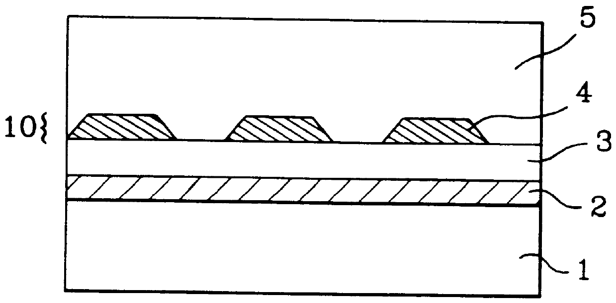
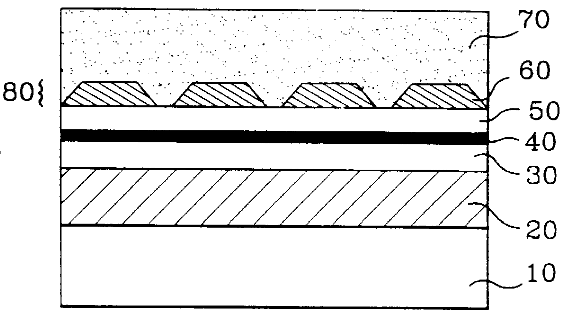
A first stage of the method consists in forming a vertical structure as shown in FIG. 2A. For this purpose, a plurality of successive layers 20, 30, 40, 50, 60 are grown epitaxially on a substrate 10 made of a III-V type material, such as InP, for example. Preferably, the substrate is made of InP that is doped with carriers of a first type, e.g. n-type carriers. Naturally, the substrate 10 may be covered with a buffer layer serving to facilitate growing of the various layers to be stacked. The buffer layer is not shown in FIG. 2A.

In the example shown in FIG. 2A, the layer 20 covering the substrate 10 constitutes a waveguide layer, also referred to as an "active layer". It is preferably made up of an alternating succession of layers of InP and of layers of a quaternary material. In one embodiment, it comprises 20 layers of InP of thickness equal to 100 .ANG. (1 .ANG.=10.sup.-10 meters) in alternation with 20 layers of quaternary material of thickness equal to 100 .ANG..

Layer 30 is ma...


PUM


Abstract

A semiconductor Bragg reflector and to a method of fabricating it. The reflector comprises a plurality of stacked layers on a substrate of a III-V type material, one of the stacked layers forming a holographic grating. The layer forming the grating comprises an alternating succession of air pockets and of III-V type material. Such a reflector is particularly suitable for use in laser devices.

Description

The present invention relates to a semiconductor Bragg reflector and a method of fabricating said reflector.Bragg reflectors are in common use in particular in the field of optical transmission. Such a reflector makes it possible to reflect a portion of the light that it receives.More particularly, a Bragg reflector is defined by a periodic grating made of two materials having different refractive indices. The reflection ratio of such a device depends both on the difference between the refractive indices of the two component materials, and also on the geometry of the grating. It is proportional to the product .kappa..times.L, where L is the length of the grating and .kappa. is the "Bragg coefficient" which is related firstly to the difference between the refractive indices of the two materials, and secondly to the thickness of the grating.A conventional reflector is shown in longitudinal section in FIG. 1A and in cross-section in FIG. 1B. For example, the reflector may be disposed f...

Claims


Application Information

Patent Timeline
IPC IPC(8): G02B6/124G02B6/13G02B6/136H01S5/12H01S5/00G02B6/12H01S5/20G02B5/08G02B5/18G02B5/32G02B6/122H01L33/30H01S5/125
CPCG02B6/124G02B6/136H01S5/12G02B2006/12107G02B2006/12176H01S5/2081
Inventor GOLDSTEIN, LEONBISSESSUR, HANSBODERE, ALAINBRILLOUET, FRAN.CEDILLA.OISGENTNER, JEAN LOUISGRAVER, CATHERINE
Owner OCLARO NORTH AMERICA
Why Eureka
Try Eureka