Emission microscope and method for continuous wavelength spectroscopy

Inactive Publication Date: 2000-03-28
INTERUNIVERSITAIR MICRO ELECTRONICS CENT (IMEC VZW)
View PDF6 Cites 30 Cited by
  • Summary
  • Abstract
  • Description
  • Claims
  • Application Information

AI Technical Summary

Benefits of technology

FIGS. 8A and 8B are position/intensity diagrams for saturated and non-saturated s

Problems solved by technology

Because the resolution of photon-emission microscopy is at best about 1 micron, localization of a defect is not usually sufficient to determine the cause of the failure or which element of a device has failed.
However, a disadvantage with filters is their relatively low transmittance and the resulting low light levels and long acquisition times for capturing the spectrum during which the DUT is biased and may deteriorate further.
This system requires two detectors and in the case where more than one emission spot is present on the DUT all the light from the emission spots will be collected and overlapping of their spectra cannot be avoided.
Further, placing any item such as the mirror c

Method used


Image

  • Emission microscope and method for continuous wavelength spectroscopy
  • Emission microscope and method for continuous wavelength spectroscopy
  • Emission microscope and method for continuous wavelength spectroscopy

Examples


first embodiment

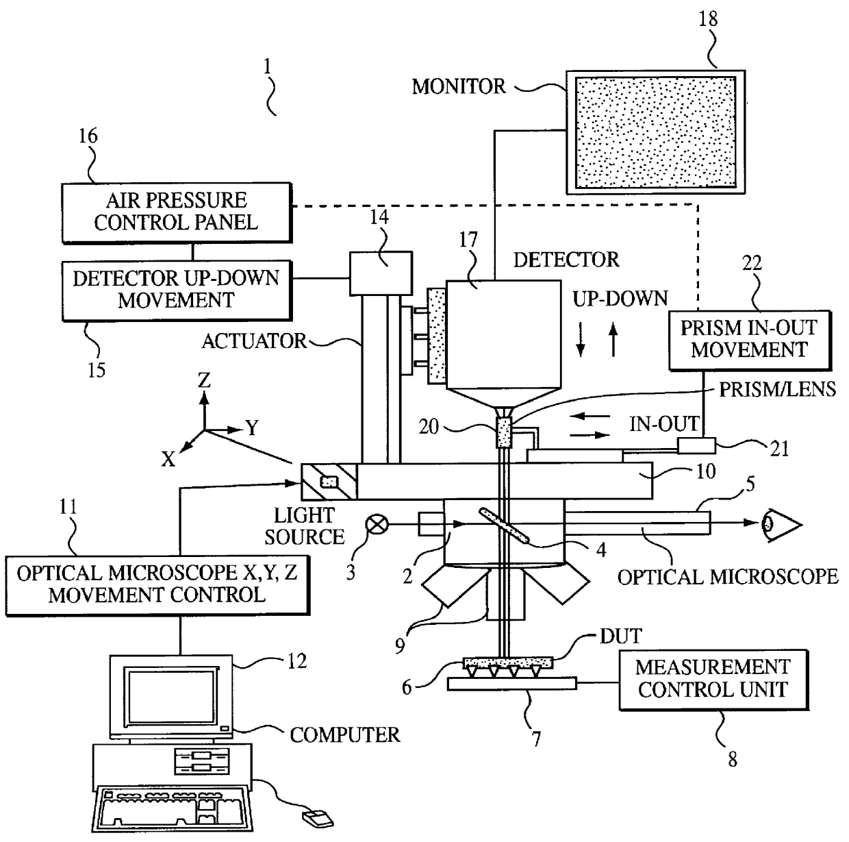
FIG. 1 is a schematic view of the microscope system 1 in accordance with the present invention. System 1 is composed of a conventional photo-emission microscope 2 (e.g. Visionary II supplied by Hypervision Inc., Fremont, Calif., USA) equipped with a highly sensitive detector 17 to which a novel high resolution spectroscopic part 20 with continuous wavelength capability is added. The detector 17 may be either an analog or digital detector, i.e. the detector 17 may be a photo-camera for recording the image from the microscope on a pbotographic film or may be a digital reproduction device capable of recording and optionally displaying the image on a suitable display screen 18. The light emitted from biased integrated circuits is very low and analog recording methods even with ultra-fast film may be too slow. Hence, it is preferred to use an image intensifier which may increase the brightness by a factor of 10,000 to 1 million or more. Image intensifier tubes can detect radiation in bot...

second embodiment

The method of operating system 1 in accordance with the second embodiment is as follows. The DUT 6 is observed with the detector 17 in the down position to roughly locate the emission spot to be measured. This may be done by observing the output of the detector 17 using the white light source 3 to illuminate the DUT 6 in order obtain a picture thereof Then the image of the DUT is observed without the white light source while the DUT is biased using the measurement and control unit 8. Once the emission spot is located, the DUT bias is preferably removed to avoid further damage to the DUT 6. The detector 17 is raised and the emission spot is again located in the field of view of the detector 17. If the mechanics of system 1 are good there should be little or no change of position of the spot location in the detector 17. The monochromator 20 is then moved into position so that it interrupts the light path from the DUT 6 to the detector 17, preferably without movement or adjustment of t...


PUM


Abstract

A photon-emission microscope method and system are described which allow both emission spot localization and continuous spectral analysis of the emited light from the emission spot of a biased electronic circuit. The system includes an emission microscope, a detector and an in-line, direct vision, chromatically dispersing prismatic device. The microscope system advantageously uses only one detector which does not need to be moved to be able to detect both the localization and spectral images. In a particular embodiment, localization of emission spots may be performed using monochromatic light which allows sharp images of the electronic circuit despite the fact that the electronic circuit is viewed through the dispersing device. Further, an improved procedure is described for overcoming errors caused by saturation of the detector at high sensitivities.

Description

The present invention relates to microscope systems for continuous wavelength spectroscopy as well as a methods of operating the same, in particular to photon-emission microscopes and microscopy. The microscope systems and methods are particularly useful in analyzing faults in electronic integrated circuits, particularly very large integrated circuits.TECHNICAL BACKGROUNDPhoton-emission microscopy is commonly used to localize failures in electronic integrated circuits. The technique detects light emitted from defects and failed elements when a device under test (DUT) is biased. Because the resolution of photon-emission microscopy is at best about 1 micron, localization of a defect is not usually sufficient to determine the cause of the failure or which element of a device has failed. Spectral analysis of the emitted light is of interest because it can provide additional information on the failure cause and place.A simple method of carrying out a spectral analysis of the emitted figh...

Claims


Application Information

Patent Timeline
IPC IPC(8): G01J3/443G01J3/12G01J3/14G01J3/28
CPCG01J3/14G01J3/2803G01J3/443
Inventor DE WOLF, INGRIDRASRAS, MAHMOUD
Owner INTERUNIVERSITAIR MICRO ELECTRONICS CENT (IMEC VZW)
Why Eureka
Try Eureka