Magnetic alignment apparatus and method for self-alignment between a die and a substrate

a technology of magnetic alignment and self-alignment, which is applied in the direction of conveyor parts, transportation and packaging, printed circuit manufacturing, etc., can solve the problems of large complexity of the alignment assembly involved, prone to breakdown, and extensive calibration

Inactive Publication Date: 2000-04-18
NAT SEMICON CORP
View PDF9 Cites 38 Cited by
  • Summary
  • Abstract
  • Description
  • Claims
  • Application Information

AI Technical Summary

Benefits of technology

Accordingly, it is an object of the present invention to provide an apparatus and method which enables self-alignment between a semiconductor die and a packaging substrate for aligned electrical connection thereof.

Problems solved by technology

Such alignment precision is achievable using current alignment technology; however, the alignment assemblies involved are substantially complex in nature, requiring extensive calibration and are prone to breakdown.
Maintenance, therefore, is relatively costly and often results in substantial down-time.
While these mechanical alignment assemblies adequately position the semiconductor die and packaging substrate for alignment purposes, one problem associated with these systems is that they are often mechanically complex involving a substantial number of moving components.
Once the cooperating components begin to wear, alignment problems occur which in turn require parts replacement and / or re-calibration.
Maintenance costs, therefore, tend to be relatively costly.
Moreover, the alignment process between the die and the substrate is typically time consuming to achieve since the substrate will be brought over to the bonding site mechanically and the alignment is also done mechanically as well before attach to the die to the substrate.
Another problem associated with these mechanical alignment systems is that the substrate may be physically damaged upon contact with the alignment system moving components.
Both optical techniques require complex circuitry, programming, and machinery to advance the optical alignment.
Thus, calibration is difficult.
These factors, hence, substantially increase fabrication and maintenance costs.
Moreover, operation speeds are relatively slow due to the difficulty of implementation, the current optical alignment technology available, as well as the precise nature of the optical alignment.

Method used


Image

  • Magnetic alignment apparatus and method for self-alignment between a die and a substrate
  • Magnetic alignment apparatus and method for self-alignment between a die and a substrate
  • Magnetic alignment apparatus and method for self-alignment between a die and a substrate

Examples


Embodiment Construction

While the present invention will be described with reference to a few specific embodiments, the description is illustrative of the invention and is not to be construed as limiting the invention. Various modifications to the present invention can be made to the preferred embodiments by those skilled in the art without departing from the true spirit and scope of the invention as defined by the appended claims. It will be noted here that for a better understanding, like components are designated by like reference numerals throughout the various figures.

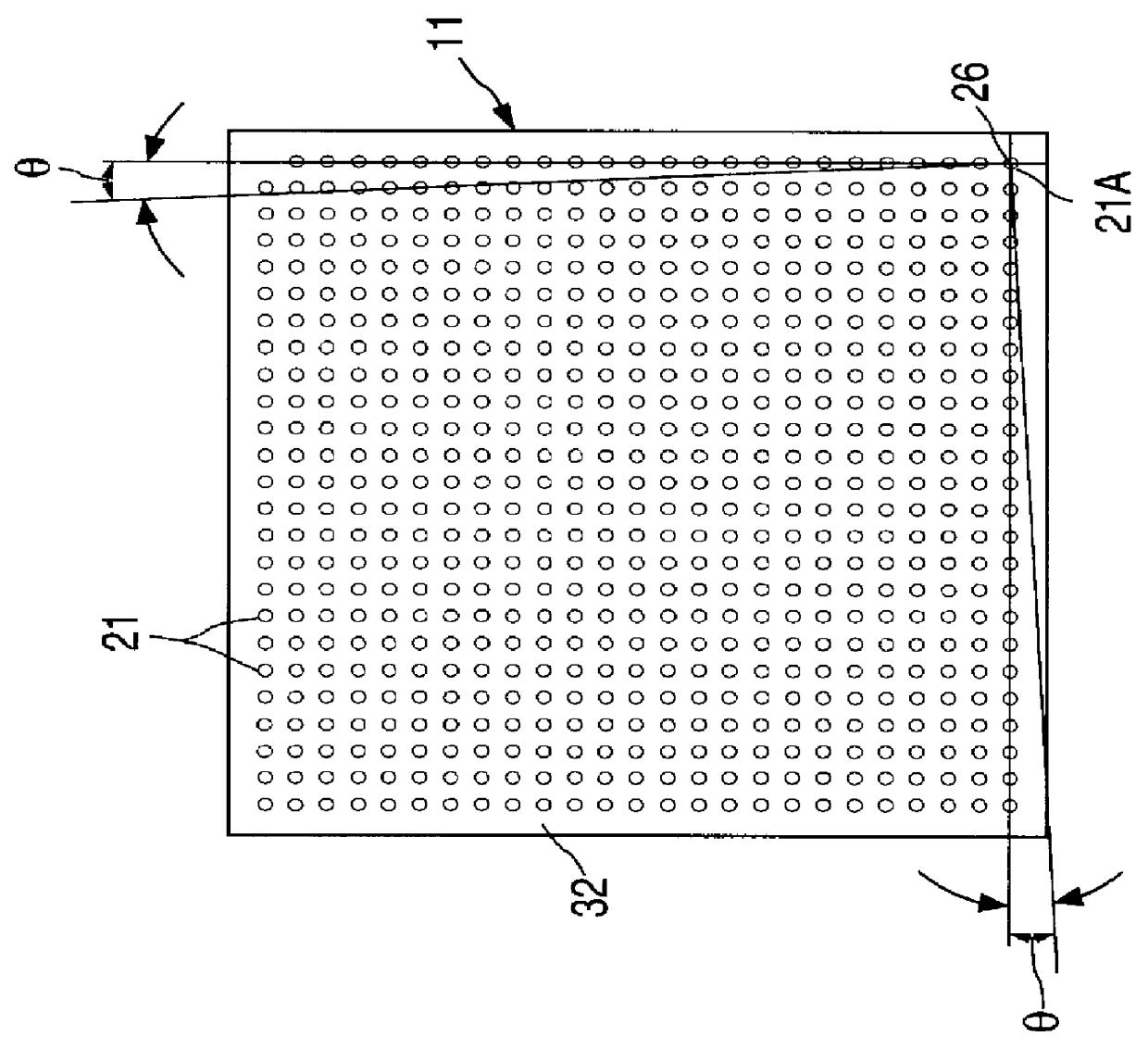
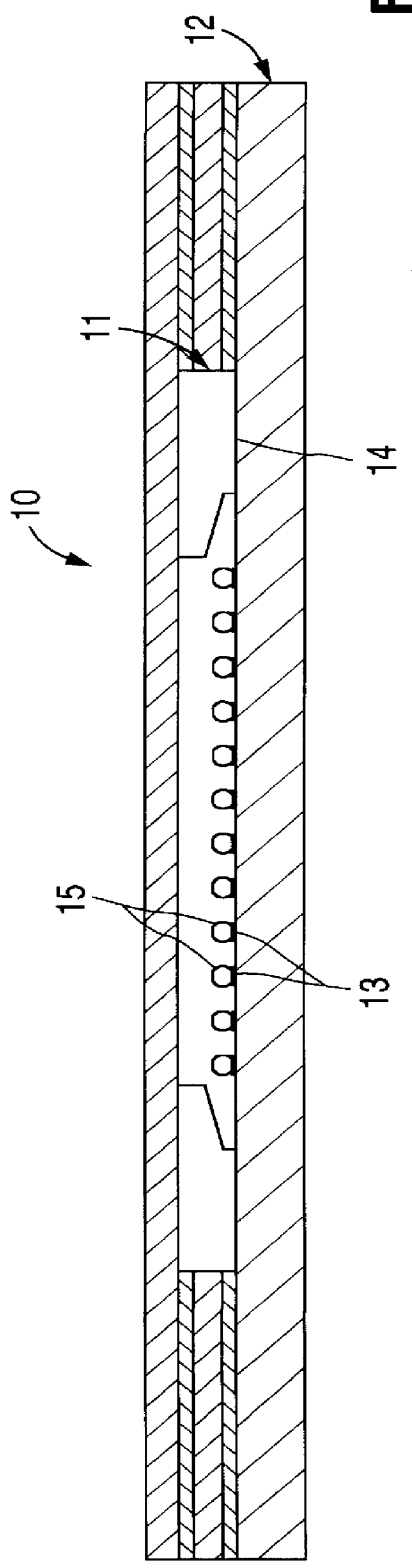
Attention is now directed to FIGS. 2A and 2B where a magnetic alignment apparatus, generally designated 20, is provided for aligning a semiconductor die 11 and a packaging substrate 12 to enable aligned electrical interconnection therebetween. More specifically, the I / O pads 21 of the semiconductor die 11 are to be aligned with the conductive traces 22 of the substrate (e.g., a Printed Circuit Board (PCB)). The alignment apparatus 20 inc...


PUM

PropertyMeasurementUnit
diameteraaaaaaaaaa
voltagesaaaaaaaaaa
magnetic fieldaaaaaaaaaa

Abstract

A magnetic alignment apparatus (20) is provided for aligning a semiconductor die (11) and a packaging substrate (12) to enable aligned mounting therebetween. The alignment apparatus (20) includes a first magnetic device (23) coupled to the die (11) and adapted to generate a first magnetic field (25) oriented relative to a first reference point (26) of the die (11). A second magnetic device (27) is coupled to the substrate (12) and adapted to generate a second magnetic field (28) oriented relative to a second reference point (30) of the substrate (12). The first magnetic field (25) and the second magnetic field (28) cooperate to directionally align the first reference point (26) of the die substantially with the second reference point (30) of the substrate (12).

Description

The present invention relates, generally, to semiconductor fabrication and, more particularly, relates to alignment apparatus for enabling alignment between semiconductor dies and packaging substrates during bonding.In semiconductor device assembly, a semiconductor chip (or "die") may be bonded directly to a packaging substrate, without the need for a separate leadframe or for separate I / O connectors (e.g. wire or tape). Such chips are typically formed with ball-shaped beads or bumps of solder affixed to their I / O bonding pads such as in a Ball Grid Array (BGA). During packaging, the chip is "flipped" onto its active circuit surface in a manner forming a direct electrical connection between the solder bumps of the chip and conductive traces on a packaging substrate. Semiconductor chips of this type are commonly referred to as "flip chips", and are advantageously of a comparatively reduced size. For example, in current flip chip designs, the semiconductor die may be dimensioned as sm...

Claims


Application Information

Patent Timeline
Patent Type & Authority Patents(United States)
IPC IPC(8): H01L21/68H01L21/67
CPCH01L21/68H01L24/95Y10T29/49131H01L2224/95122H01L2224/95144H01L2924/01029H01L2924/01039H01L2924/01075H01L2924/19041H01L2924/19042H01L2924/19043H01L2924/3011H01L2924/01005H01L2924/01006H01L2924/01023H01L2924/01033Y10T29/4913
Inventor ASANASAVEST, CHAINARONG
Owner NAT SEMICON CORP
Why Eureka
Try Eureka