
Geometric phase analysis for mask alignment

a technology of phase analysis and mask alignment, applied in the field of geometric phase analysis for mask alignment, can solve the problems of insufficient future generations of integrated circuits, poor performance, and the critical problem of measuring the misalignment between features formed in different layers

Inactive Publication Date: 2000-05-09
GLOBALFOUNDRIES INC
View PDF5 Cites 56 Cited by
  • Summary
  • Abstract
  • Description
  • Claims
  • Application Information

AI Technical Summary

Problems solved by technology

Therefore, the problem of measuring the misalignment between features formed in different layers has become more critical.
This accuracy is sufficient for present day needs but will be inadequate for future generations of integrated circuits with smaller feature sizes requiring more precise alignment.
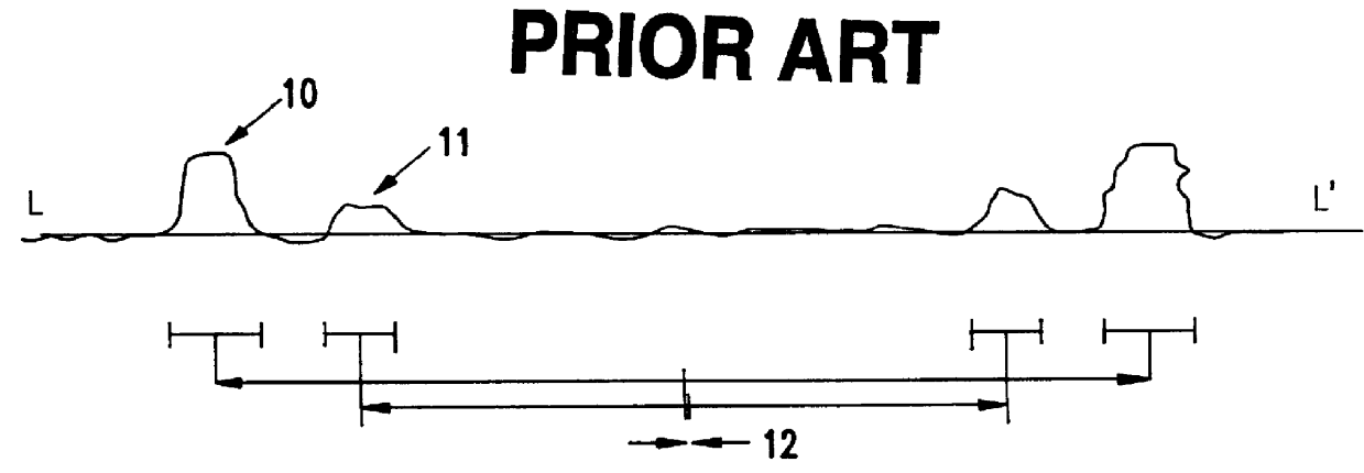
For these smaller circuits, yield problems occur when the conventional technique measures an acceptable overlay error and allows the wafer to be fully processed, but it is later found that there is poor performance due to an overlay error smaller than can be resolved using the technique.
A separate problem of the conventional technique is that it relies on measurements of large alignment marks, several microns in size, whereas the features in the actual circuits are much smaller, of the order of 250 nm (or 0.25 microns).
However, since the processing is optimized for the smaller features in the circuit, the edges of the large alignment marks may be improperly etched, making it difficult to measure their positions.
More importantly, it may be difficult to relate the position of the large alignment marks to the positions of the small features in the actual circuits, because large and small features are etched at different rates during processing.
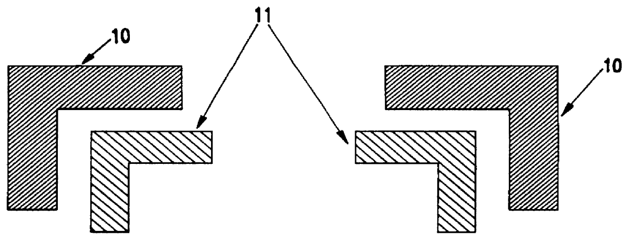
However, other significant problems occur with moire fringe techniques.
This can distort the level "B" pattern and make it difficult to expose and develop correctly.
A second problem is that the level "B" pattern shows very weak contrast (since it is only patterned in photoresist) compared to level "A" (which is etched onto the wafer).
When superimposed onto the high contrast level "A" pattern, level "B" is very difficult to see, making the moire fringes weak and the measurement less precise.
A third problem is that the difference in spacing between levels "A" and "B" must be small (around 1%) and carefully controlled in order to get appropriate moire fringes and this can be difficult to achieve.

Method used


Image

  • Geometric phase analysis for mask alignment
  • Geometric phase analysis for mask alignment
  • Geometric phase analysis for mask alignment

Examples


Embodiment Construction

Referring now to the drawings, the inventive technique for the measurement of overlay error using geometric phase analysis is illustrated. The discussion of the invention begins by describing the alignment marks which are used in this technique, and then describes mathematical calculations, using the technique of geometric phase analysis, with which the overlay error can be measured from these alignment marks.

FIG. 2A shows the alignment marks used in the present technique, which consist of regular arrays of small dots or other features. The alignment marks are formed in an alignment area which is separate from the wiring pattern area of the masks.

At the first mask level, referred to hereafter as level "A", an alignment mark (labeled 20 in FIG. 2A) is etched into the wafer. In a preferred embodiment, this alignment mark comprises an array of 10.times.20 small dots, each dot being 550 nm across with a spacing between dots of 550 nm. Therefore, in the example illustrated, the level "A"...


PUM


Abstract

A method of measuring overlay error comprises forming a first mask having a first alignment array comprising a periodic pattern of first features having a first periodicity, forming a second mask having a second alignment array comprising a pattern of second features having the first periodicity, the first alignment array being adjacent the second alignment array, the first alignment array and the second alignment array forming a combined alignment array, transforming the combined alignment array to produce a transformed array, selecting a first region within the transformed array, inverse transforming the region to produce geometric phase shift information, averaging the phase shift information, converting the averaged phase shift information into a value for misalignment in a first direction corresponding to the first region, repeating the selecting, inverse transforming, averaging and converting using a second region within the transformed array to calculate a value for misalignment in a second direction corresponding to the second region, calculating an overlay error between the first and second mask levels by adding the components of misalignment in the first direction and second direction.

Description

1. Field of the InventionThe present invention generally relates to methods for measuring the misalignment, or overlay error, between the patterns created on a wafer in different steps of the integrated circuit manufacturing process, and more specifically to improved methods of measuring misalignment which utilize geometric phase analysis.2. Description of the Related ArtDuring the process of integrated circuit fabrication, several hundred processing steps may be required as thin layers of semiconductors, insulators and metals are deposited and patterned. The patterns in each layer of the integrated circuit are created using the process of lithography. A photosensitive resist ("photoresist") is deposited on the silicon wafer and exposed to light through a mask carrying the desired pattern. The photoresist is then developed and removed from areas corresponding to the pattern, allowing the pattern to be transferred by etching into the layer below.With every generation of smaller and f...

Claims


Application Information

Patent Timeline
IPC IPC(8): G03F7/20G06T7/00
CPCG03F7/70633G06T7/001G06T7/0036Y10S345/953G06T2207/30148G06T7/37
Inventor ROSS, FRANCES MARY
Owner GLOBALFOUNDRIES INC
Learn More