Synchronous semiconductor memory device having redundant circuit of high repair efficiency and allowing high speed access

a synchronous semiconductor and memory device technology, applied in the direction of information storage, static storage, digital storage, etc., can solve the problems of reducing the repair efficiency of redundancy replacement, unable to obtain sufficient operational margin, and increasing the penalty for affecting the operation of the device, so as to achieve sufficient operational margin, speed up access time, and suppress the effect of increasing power consumption

Inactive Publication Date: 2000-05-23
MITSUBISHI ELECTRIC CORP
View PDF7 Cites 67 Cited by
  • Summary
  • Abstract
  • Description
  • Claims
  • Application Information

AI Technical Summary

Benefits of technology

A main advantage of the present invention is that a sufficient operational margin can be obtained and that the access time can be speeded up even when redundancy replacement is carried out since the first and second column select circuit operate in parallel.
is that a sufficient operational margin can be obtained and that the access time can be speeded up even when redundancy replacement is carried out since the first and second column select circuit operate in parallel.
Another advantage of the present invention is that increase in power consumption can be suppressed even when redundancy replacement is carried out since the subamplifier operates when the redundant column is selected.
A further advantage of the present invention is that a redundant memory cell block can be replaced with any of the first plurality of regular memory cell blocks, and that the repair efficiency is high and increase in chip area can be suppressed in a synchronous semiconductor memory device integrated in high complexity.

Problems solved by technology

There is a problem that the area penalty is increased by incorporating any extra redundant row (column), or that the repair efficiency by redundancy replacement is reduced.
In a SDRAM that must carry out operation at high speed, there was a problem that a sufficient operational margin could not be obtained when redundancy replacement is carried out since extra time is necessary to determine whether or not to effect redundancy replacement with respect to an externally applied address signal.
There was also a problem that the operating current and power consumption during standby are increased in accordance with a larger storage capacity of the memory.

Method used


Image

  • Synchronous semiconductor memory device having redundant circuit of high repair efficiency and allowing high speed access
  • Synchronous semiconductor memory device having redundant circuit of high repair efficiency and allowing high speed access
  • Synchronous semiconductor memory device having redundant circuit of high repair efficiency and allowing high speed access

Examples


first embodiment

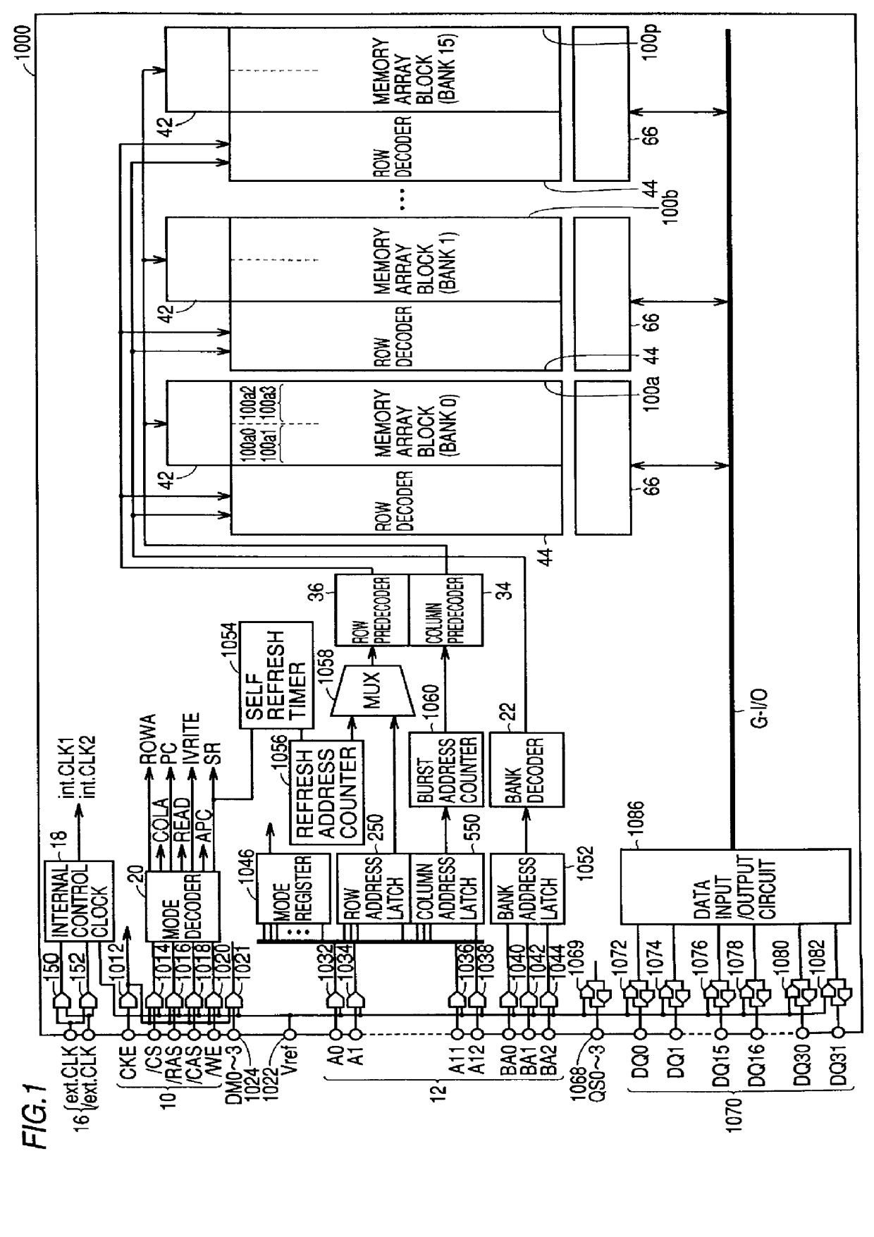
FIG. 1 is a schematic block diagram showing the concept of the structure of a synchronous semiconductor memory device 1000 according to a first embodiment of the present invention.

SDRAM 1000 includes an external clock signal input terminal 16 receiving externally applied complementary clock signals ext.CLK and ext. / CLK, clock input buffers 150 and 152 for buffering the clock signal applied to external clock terminal 16, an internal control clock signal generation circuit 18 receiving the outputs of clock buffers 150 and 152 to generate a first internal clock signal int.CLK1 and a second internal clock signal int.CLK2, and a mode decoder 20 receiving via input buffers 1012-1020 operating according to second internal clock signal int.CLK2 an external control signal applied via external control signal input terminal 10.

Second internal clock signal int.CLK2 is a signal having a frequency identical to that of external clock signal ext.CLK. First internal clock signal int.CLK1 is a signal...

second embodiment

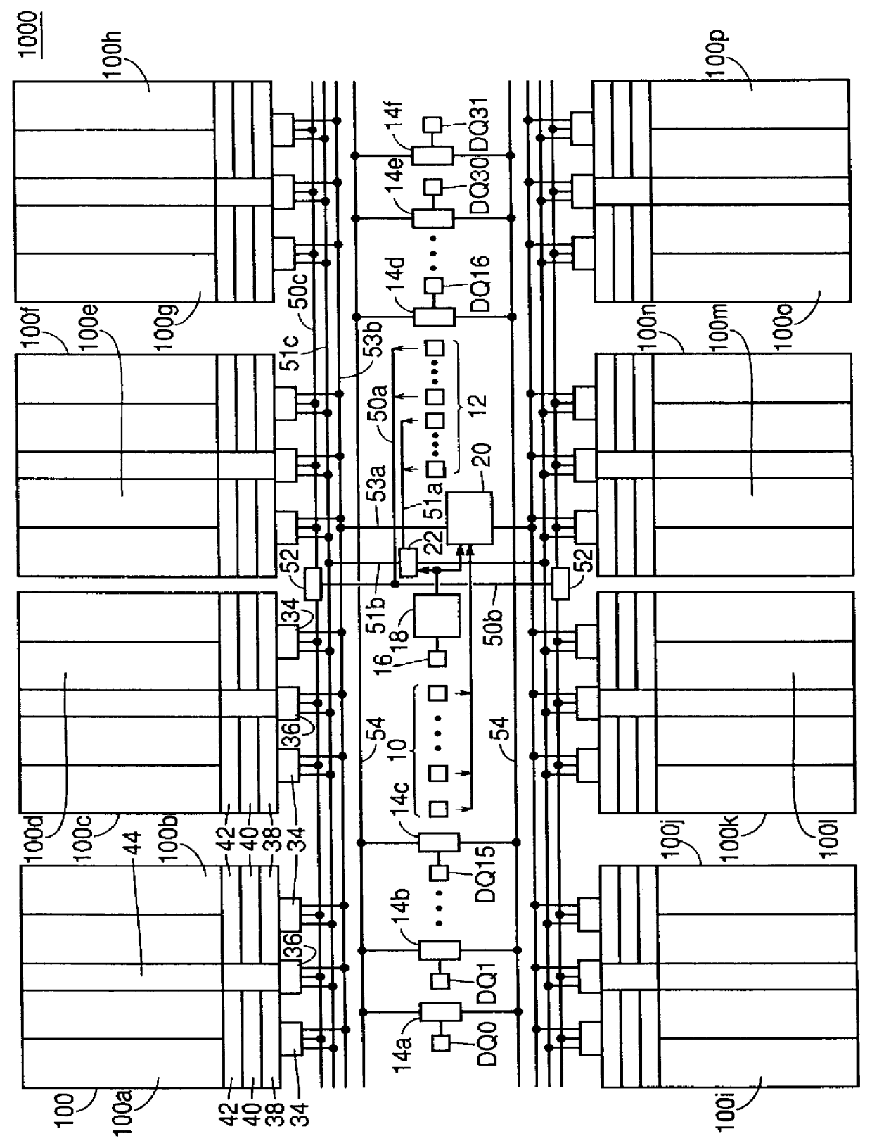
FIG. 23 is a schematic block diagram showing a structure of a sub I / O line pair, a main I / O line pair, a main amplifier, a multiplexer, and a global I / O line pair G-I / O according to a second embodiment of the present invention.

The structure of FIG. 23 is comparable to the structure of FIG. 11. The structure of FIG. 23 differs from the structure of FIG. 11 in that a multiplexer 644 is provided in the path from main amplifiers 602-608 corresponding to the regular memory cell column to the global I / O bus in, for example, region 100a0.

The remaining elements are similar to those of the structure of the first embodiment shown in FIG. 11. Corresponding components have the same reference characters allotted, and their description will not be repeated.

The load and the like in the data transfer path is equalized in both the regular memory cell column side and the redundant memory cell column side according to the structure of FIG. 23 to allow improvement of the operation balance therebetween....

third embodiment

FIG. 24 is a circuit diagram showing a structure of a transfer gate portion to transmit data from a selected bit line pair to a sub I / O line pair RS-I / O in a redundant memory cell column region SR0 in a synchronous semiconductor memory device according to a third embodiment of the present invention. FIG. 24 is comparable to FIG. 13 of the first embodiment.

In FIG. 24, only the structure of the portion connected to two line pair RS-I / O corresponding to two memory cell columns by one column select line is illustrated.

In practice, four bit line pairs are connected to four corresponding sub I / O line pairs RS-I / O by the activation of one column select signal.

Referring to FIG. 24, activation of column select line RYS0 causes the pair of bit lines BL0 and ZBL0 to be connected to sub I / O line pair RS-I / O0 via transfer gate transistors TN01 and TN02, respectively.

In contrast, bit line pair BL1 and ZBL1 is connected to sub I / O line pair RS-I / O1 via transfer gate transistors TN11 and TN12, resp...


PUM


Abstract

A redundant memory cell column region provided corresponding to respective regular memory cell column regions can have data read and written through a sub I / O line pair and a main I / O line pair independent to those of the regular memory cell column region. Also, one redundant memory cell column region can be connected to a corresponding global I / O line pair G-I / O of any of the regular memory cell column regions via a multiplexer to be replaceable of any of two regular memory cell column regions.

Description

BACKGROUND OF THE INVENTION1. Field of the InventionThe present invention relates to synchronous semiconductor memory devices, and more particularly, to the structure of a redundant circuit in a synchronous semiconductor memory device.2. Description of the Background ArtIn order to comply with the higher operation speed of recent microprocessors (referred to as MPU hereinafter), a synchronous DRAM (referred to as SDRAM hereinafter) is used that operates in synchronization with a clock signal to realize high speed access of a dynamic random access memory (referred to as DRAM hereinafter) employed as a main storage device. Control of the internal operation of such SDRAMs is carried out with the row related operation and the column related operation separated from each other.In order to further increase the operation speed in a SDRAM, a bank structure is employed in which the memory cell array is divided into a plurality of banks that can operate independent of each other. In other wor...

Claims


Application Information

Patent Timeline
Patent Type & Authority Patents(United States)
IPC IPC(8): G11C29/00G11C11/407G11C11/401G11C11/409G11C29/04
CPCG11C29/842G11C29/808
Inventor OOISHI, TSUKASATOMISHIMA, SHIGEKISHIMANO, HIROKI
Owner MITSUBISHI ELECTRIC CORP
Why Eureka
Try Eureka