
Semiconductor memory device with a voltage down converter stably generating an internal down-converted voltage

a technology of semiconductor memory devices and voltage converters, which is applied in the direction of digital storage, differential amplifiers, instruments, etc., can solve the problems of overshooting of internal power supply voltage vci, unstable operation of load circuit 7, and increased consumption current of semiconductor devices

Inactive Publication Date: 2000-06-06
RENESAS ELECTRONICS CORP
View PDF12 Cites 63 Cited by
  • Summary
  • Abstract
  • Description
  • Claims
  • Application Information

AI Technical Summary

Problems solved by technology

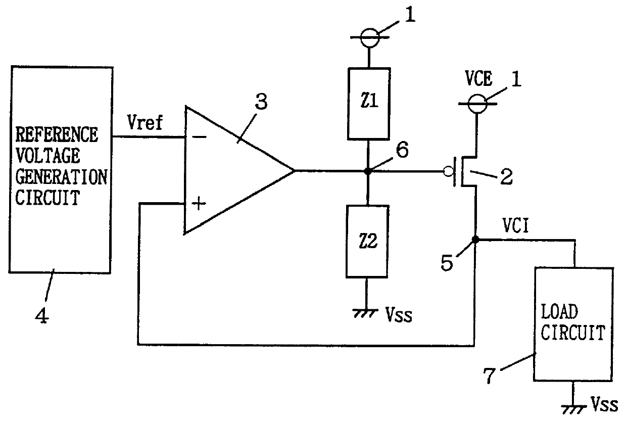
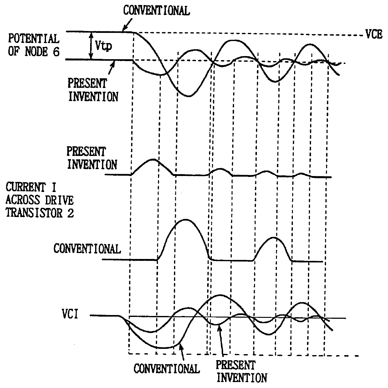
As a result, overshooting occurs in internal power supply voltage VCI.
Therefore, a stable operation of load circuit 7 cannot be ensured.
Repetition of overshooting / undershooting causes a longer time period of the current supply through drive transistor 2, inducing a problem that the consumed current of the semiconductor device is increased.
The time period of the flow of a great current is lengthened due to delay in the response of adjustment in the feedback loop, resulting in the problem that power consumption of the semiconductor device is increased.
Thus, the above-described problem of delay in response becomes significant.
Furthermore, when load circuit 7 operates and internal power supply voltage VCI changes abruptly, drive transistor 2 will be turned on in a delayed manner due to the delay in the response.
The above-described problem occurs, not only in an internal voltage down converter, but also in a feedback control system that feeds back an output signal that is to be maintained at a predetermined voltage level to a comparison circuit for controlling the level of the output signal according to the output signal fed back to the comparison circuit.
The voltage of the power supply node is varied due to this consumed current, resulting in generation of a power supply noise.
Here, the level of the input and output signals of other circuits to which the current from that power supply node is provided are varied according to a change in the voltage of this power supply node, resulting in a problem that an erroneous operation is generated in the other circuits.
As a result, sense operation cannot be carried out at high speed.
Furthermore, when this voltage change of the power supply node is great, the logic on the bit line is erroneously detected to cause an erroneous sensing operation.
Furthermore, the limitation of the amplitude allows an output signal of the comparison circuit to speedily change according to a change of the voltage of the first node.
Furthermore, this restore operation is time consuming.
In the case of load circuit 7B such as a sense amplifier that charges / discharges a bit line, current consumption is great since there are a great many number of bit lines to be charged.
Therefore, in this region, amplitude limitation of an output signal of comparison circuit is not carried out.
Amplitude limitation is carried out only when the output signal has a great amplitude.

Method used


Image

  • Semiconductor memory device with a voltage down converter stably generating an internal down-converted voltage
  • Semiconductor memory device with a voltage down converter stably generating an internal down-converted voltage
  • Semiconductor memory device with a voltage down converter stably generating an internal down-converted voltage

Examples


tenth embodiment

FIG. 64 shows a second specific structure of an internal power supply voltage generation circuit according to the present invention. Referring to FIG. 64, an adjustment circuit 310 includes a p channel MOS transistor 315 provided between external power supply node 1 and drive element 60. The potential of node D is supplied to the gate of MOS transistor 315. The other components are similar to those shown in FIG. 47, and corresponding components have the same reference characters denoted. The operation thereof will be described.

Similar to the structure shown in FIG. 61, the charged potential of loop filter 309 (the potential of node D) corresponds to the integrated value of the prior cycle (the operation cycle of load circuit 7) with reference to reference voltage Vref of internal power supply voltage VCI. When the amount of undershooting of internal power supply voltage VCI is greater than the amount of overshooting, the potential of node D is lowered. In contrast, when the amount o...

embodiment 11

FIG. 65 shows the entire structure of a semiconductor memory device in which an internal voltage down converter is applied according to an eleventh embodiment of the present invention. Referring to FIG. 65, a semiconductor memory device includes four memory cell arrays 102a, 102b, 102c and 102d arranged on a semiconductor chip 100. Each of memory cell arrays 102a-102d includes a plurality of memory cells arranged in a matrix of rows and columns, a bit line pair disposed corresponding to each column, a word line disposed corresponding to each row, and a sense amplifier provided corresponding to each bit line pair. The method of selecting a memory cell from memory cell arrays 102a-102d is appropriately selected. A structure may be employed where a predetermined number of memory cells (for example 1 bit) is selected in each of memory cell arrays 102a-102d in an access mode. Furthermore, a structure may be employed where a predetermined number of arrays (for example, memory cell arrays ...

modification 1

[Modification 1]

FIG. 71 shows a first modification of an array internal voltage down converter. Referring to FIG. 71, an array internal voltage down converter includes an active internal voltage down converter 242 for adjusting the voltage level of internal power supply voltage on internal power supply line 245a at an active state, an active internal voltage down converter 244 for adjusting the voltage level of internal power supply voltage VCIb on internal power supply line 245b when active, and a constant internal voltage down converter 247 for adjusting the voltage level of internal power supply voltages VCIa and VCIb on internal power supply lines 245a and 245b, respectively. Internal power supply lines 245a and 245b may be formed of different interconnections or of the same interconnections. More specifically, a structure is provided where internal power supply lines 245a and 245b supply internal power supply voltages VCIa and VCIb to different memory cell arrays. The voltage l...


PUM


Abstract

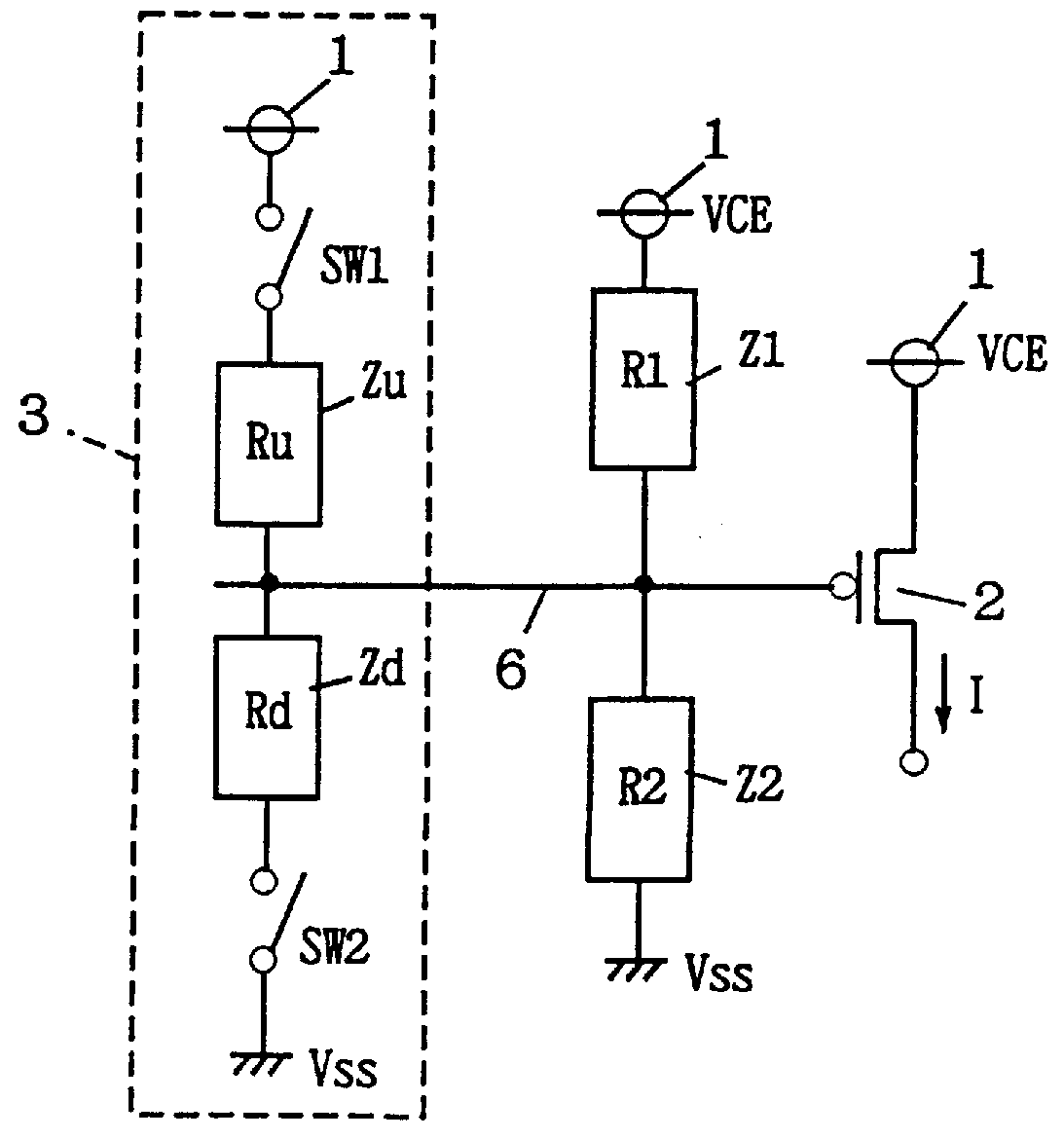
A comparison circuit compares a reference voltage Vref from a reference voltage generation circuit with an internal power supply voltage VCI on an internal power supply line to provide a signal according to the comparison result. A drive transistor supplies current to the internal power supply line from an external power supply node according to the output signal of the comparison circuit. A resistance element connected between the external power supply node and the output node of the comparison circuit and a resistance element connected between the output node of the comparison circuit and a ground node VSS suppresses the amplitude of an output signal of the comparison circuit. Thus, overdrive of the drive transistor can be suppressed, and a current corresponding to an abrupt change of the internal power supply voltage can be supplied from the external power supply node to the internal power supply line by the amplitude limitation function. Thus, an internal power supply voltage generation circuit is provided superior in high frequency response that can generate an internal power supply voltage stably.

Description

1. Field of the InventionThe present invention relates to semiconductor memory devices, and more particularly, to a structure for maintaining an internal node, to which voltage of a constant level is transmitted, at a constant voltage level stably. More particularly, the present invention relates to a structure of an internal voltage down converter for down-converting an external power supply voltage to generate an internal power supply voltage.2. Description of the Background ArtThe size of elements in a semiconductor memory device which are the components thereof is reduced in accordance with increase in the density and degree of integration. The internal operating power supply voltage is decreased to improve reliability of such miniaturized elements, to increase the operation speed due to reduction in the signal amplitude on a signal line, and to reduce power consumption. In contrast, miniaturization is not so advanced in processors and logic LSIs (Large Scale Integrated circuit)...

Claims


Application Information

Patent Timeline
Patent Type & Authority Patents(United States)
IPC IPC(8): G11C11/4074G11C11/407G11C11/409G05F1/56G05F3/24G11C5/14G11C11/403G11C11/408H03F3/45
CPCG11C5/143G11C11/4074G11C5/147
Inventor OOISHI, TSUKASA
Owner RENESAS ELECTRONICS CORP
Learn More