3-D CMOS-on-SOI ESD structure and method

a three-dimensional, soi-based technology, applied in the direction of semiconductor devices, diodes, electrical apparatus, etc., can solve the problems of gate resistance, channel profiling and other barriers, gate resistance, sce control, gate resistance, etc., and achieve the effect of improving the control of manufacturing and power consumption, reducing the difficulty of dealing with short-channel effects and other barriers

Inactive Publication Date: 2000-06-13
IBM CORP
View PDF19 Cites 99 Cited by
  • Summary
  • Abstract
  • Description
  • Claims
  • Application Information

AI Technical Summary

Problems solved by technology

However, with power supply reduction, transistor performance is severely impacted by both junction capacitance and the MOSFET body effect at lower voltages.
As technologies scale below 0.25-.mu.m channel lengths, to 0.15 and 0.1 .mu.m, short-channel effects (SCE) control, gate resistance, channel profiling and other barriers become an issue for advanced CMOS technologies.
While significant success has been achieved with successive scaling of bulk CMOS technology, the manufacturing control issues and power consumption will become more difficult with which to deal.
SOI has not become a mainstream CMOS technology in view of the rapid improvement in bulk CMOS technology performance, however, SOI is a contender for mainstream CMOS applications.
One of the barriers to implementing SOI as a mainstream CMOS technology is the "floating body" issue.
With respect to ESD protection, one problem with SOI is that there are no diodes natural to the process that are not in the presence of a polysilicon gate edge.
In early SOS / SOI literature, SOS and SOI were regarded as costly, having low volume, and capable of exotic applications where ESD robustness was more of a curiosity than a manufacturing necessity or supplier objective.
Disadvantages of SOI ESD networks formed solely in the SOI layer include: 1) high thermal impedance to the bulk substrate, 2) thin films, 3) polysilicon gate structures, and 4) a lack of vertical silicon diodes.
A high thermal impedance creates high surface temperatures in an SOI film thereby leading to thermal secondary breakdown in SOI devices formed in the SOI film.
Thin film SOI devices also lead to an existence of high current densities, thus creating significant power / density constraints.
In thin film SOI devices, the polysilicon gate structures create the existence of high capacitance structures and are prone to electrical overload and dielectric breakdown.
A lack of vertical structures in SOI devices prevents electrical current from being dissipated to the underlying bulk substrate and thus forces construction of wide perimeter lateral structures.
As a result, negative pulse SOI ESD protection is as difficult to provide as positive pulse SOI ESD protection.
In bulk silicon, using comparatively smaller structures, ESD protection for negative mode pulses is easily achieved because of current dissipation to the bulk substrate; whereas, in SOI this is not true.
One problem with thin film SOI ESD devices, however, is that SOI-based ESD circuits are worse than bulk devices by at least a factor of two (2.times.).
To therefore attain a robustness comparable with bulk ESD protection then will require very large SOI ESD networks which will be unacceptable in size, or capacitance loading.
Another problem in the art is that the known SOI ESD structures are all MOSFET based.
The above mentioned SOI ESD structures all disadvantageously introduce a polysilicon gate structure.
The alternatives to SOI ESD protection, as discussed above, are unacceptable from a reliability and a functional perspective.
The method of Kawai thus disadvantageously requires additional semiconductor chip area devoted to the bulk transistors, as well as, introduces undesirable topography concerns.
In other words, the method and structure taught by Kawai introduces a significantly varied topography, which would be unacceptable for high density and planarity integration applications.
While the teaching of Sun eliminates planarity concerns, it however leads to undesirable silicon dislocations, which are highly unacceptable from a manufacturing perspective.
The latter, however, introduces an area disadvantage.
Whereas the proposed solutions thus far discussed solve the concern of building ESD networks in the thin SOI film, they do not resolve semiconductor manufacturing problems, yield and topography issues.
In the above discussed related art, no ESD solution has been proposed that uses ESD structures under active circuitry of a CMOS-on-SOI structure to eliminate the problem of an excessive consumption of semiconductor chip area.
The solutions, as discussed above, are unacceptable from a reliability and functional perspective.

Method used


Image

  • 3-D CMOS-on-SOI ESD structure and method
  • 3-D CMOS-on-SOI ESD structure and method
  • 3-D CMOS-on-SOI ESD structure and method

Examples


Embodiment Construction

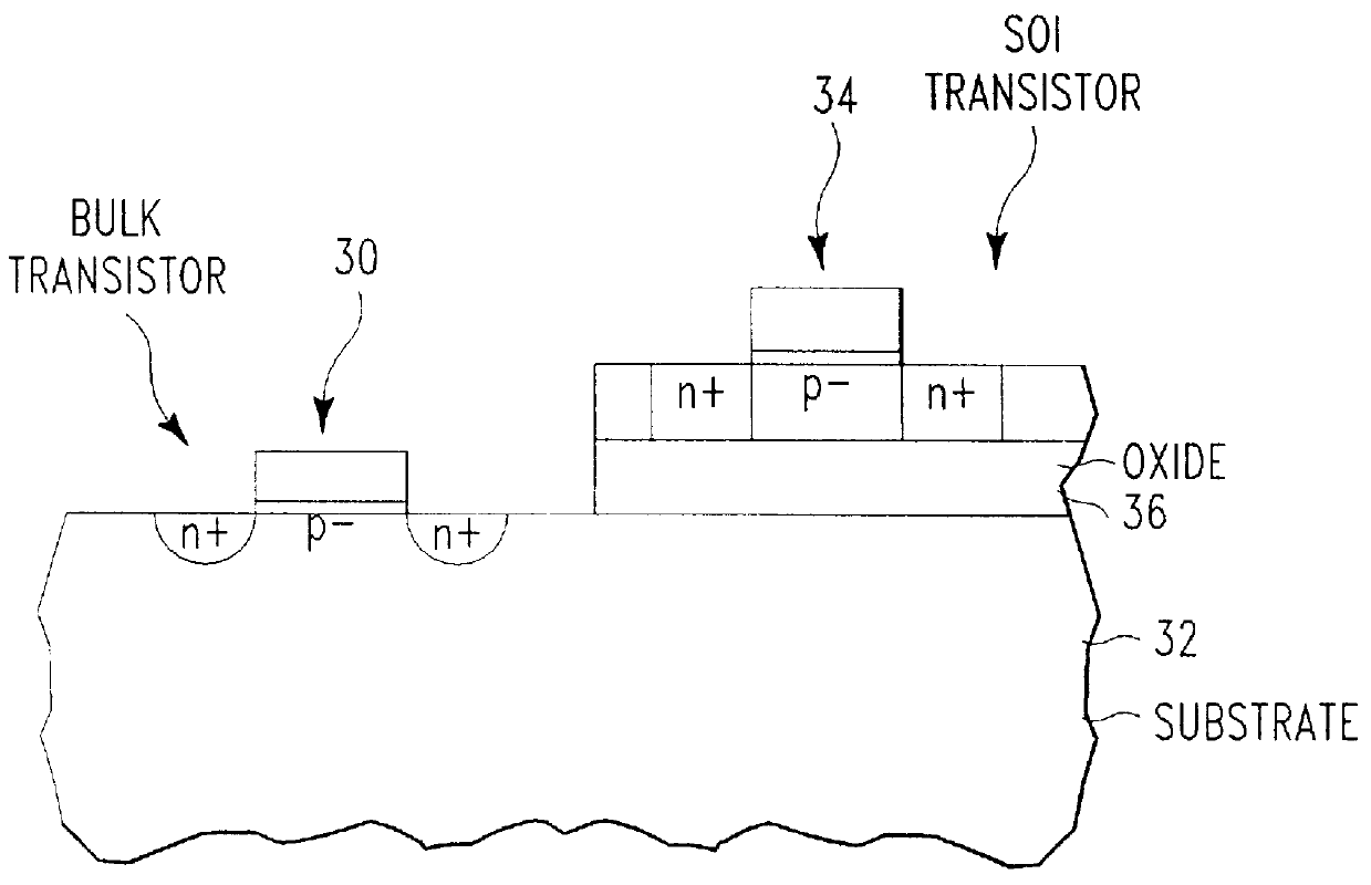
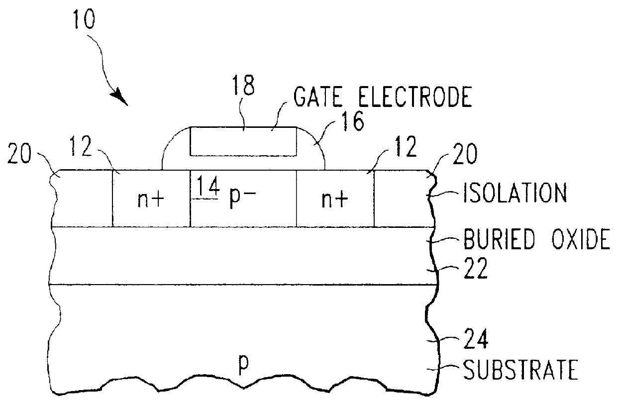
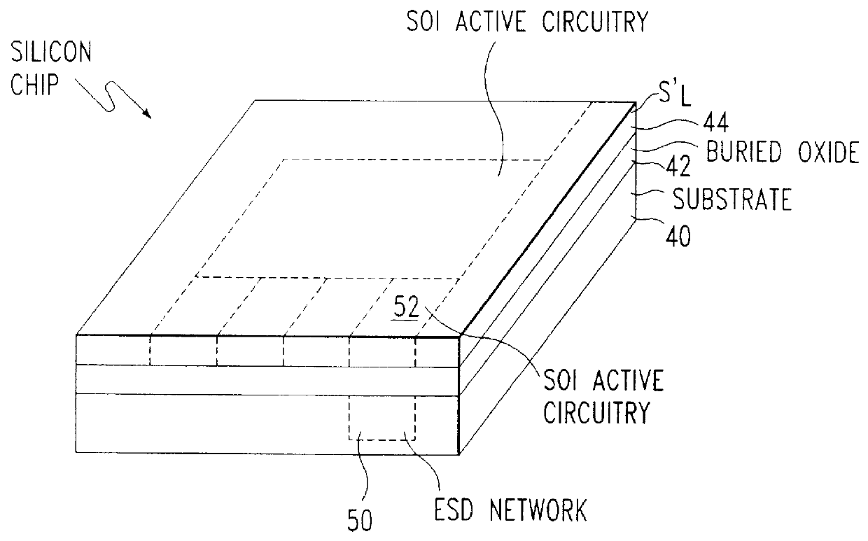
Turning now to the FIGS. 3 and 4, the three-dimensional (3-D) CMOS-on-SOI (Complementary-Metal-Oxide-Semiconductor on Silicon-on-Insulator) electrostatic discharge (ESD) structure according to the present invention includes a bulk substrate 40, a buried oxide layer 42, a thin silicon film 44, an active core structure in the thin silicon film, and an ESD structure placed under the active core structure. FIG. 3 shows a floor plan of bulk ESD networks 50 under SOI active core circuitry 52 in accordance with one embodiment of the present invention. In addition, FIG. 4 shows a floor plan of bulk ESD elements 60 under SOI ESD element circuitry 62 in accordance with another embodiment of the present invention.

In a preferred embodiment according to the present invention, the CMOS-on-SOI technology applies to a low voltage logic technology on the order of less than 5 volts. Structural features of the thin film portions of the ESD structures according to the present invention are defined by s...


PUM


Abstract

Three-dimensional ESD structures are constructed in SOI technology that utilize both bulk devices and thin film SOI devices.

Description

1. Field of the InventionThis invention relates generally to a method and apparatus for electrostatic discharge (ESD) protection in silicon-on-insulator (SOI) technologies and, more particularly, to a three-dimensional (3-D) ESD SOI structure.2. Discussion of the Related ArtMetal oxide semiconductor field effect transistor (MOSFET) scaling on bulk silicon has been the primary focus of the semiconductor and microelectronic industry for achieving complementary metal oxide semiconductor (CMOS) chip performance and density objectives. The shrinking of MOSFET dimensions for high density, low power and enhanced performance requires reduced power-supply voltages. Because power consumption (P) is a function of capacitance (C), power supply voltage (V), and transition frequency (f), in accordance with the expression P=CV.sup.2 f, the focus has been on reducing both C and V as the transition frequency f increases. As a result, dielectric thickness and channel length are scaled with power-supp...

Claims


Application Information

Patent Timeline
IPC IPC(8): H01L27/12H01L27/02
CPCH01L27/0255H01L27/1203H01L27/0259
Inventor VOLDMAN, STEVEN HOWARD
Owner IBM CORP
Why Eureka
Try Eureka