Method for producing a pn-junction for a semiconductor device of SiC

a semiconductor device and pn-junction technology, applied in the direction of semiconductor devices, basic electric elements, electrical apparatus, etc., can solve the problems of severe stress on the material, diffusion technique is not suited as a processing technique for sic, and cannot be used under altered conditions

Inactive Publication Date: 2000-07-04
CREE INC
View PDF1 Cites 85 Cited by
  • Summary
  • Abstract
  • Description
  • Claims
  • Application Information

AI Technical Summary

Problems solved by technology

However, some of the techniques used to produce semiconductor devices of other materials, such as Si, may not be used or only used under altered conditions for SiC.
Accordingly, the diffusion technique is not suited as a processing technique for SiC.
However, a SiC-layer subjected to implantation has to be kept at a temperature in the range of e.g. 500-1000.degree. C. during the implantation step putting severe stresses on the material used for a mask for the implantation.
Another problem is that it is difficult to etch away a layer of SiC on another SiC-layer and stop the etching when reaching the SiC-layer, since the etching process may not by itself stop when it reaches the SiC-layer.
The main problem of the methods already known of the type defined in the introduction is that too many mask layers have to be used in the method, and the time needed for carrying out such a method is almost directly proportional to the number of mask layers, so that such a device will be comparatively costly.
This can sometimes completely destroy the mask during implantation and thus the anode will be implanted in the wrong place.
Furthermore, due to the high temperature during implantation it is very difficult to achieve a clean surface after the mask has been removed.
As stated above, it is not possible to stop the etching process at a certain plane, such as the plane of the interface of the first and second layers, in SiC, which in combination with the fact that the thickness of the layer of SiC epitaxially grown varies for different wafers of SiC makes it necessary to measure the thickness of the layer epitaxially grown for each wafer for determining the etch depth individually for each wafer, which of course constitutes a costly procedure.
If on the other too much material is etched away, after the subsequent implantation into the second layer for forming the junction termination zones it will not be possible to obtain any contact between these zones and the main zone of the pn-junction, so that the device will not be able to hold a voltage being high enough when reverse biased.

Method used


Image

  • Method for producing a pn-junction for a semiconductor device of SiC
  • Method for producing a pn-junction for a semiconductor device of SiC
  • Method for producing a pn-junction for a semiconductor device of SiC

Examples


Embodiment Construction

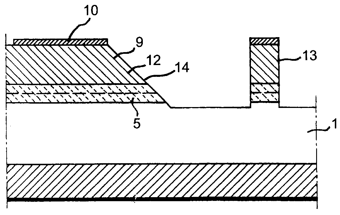
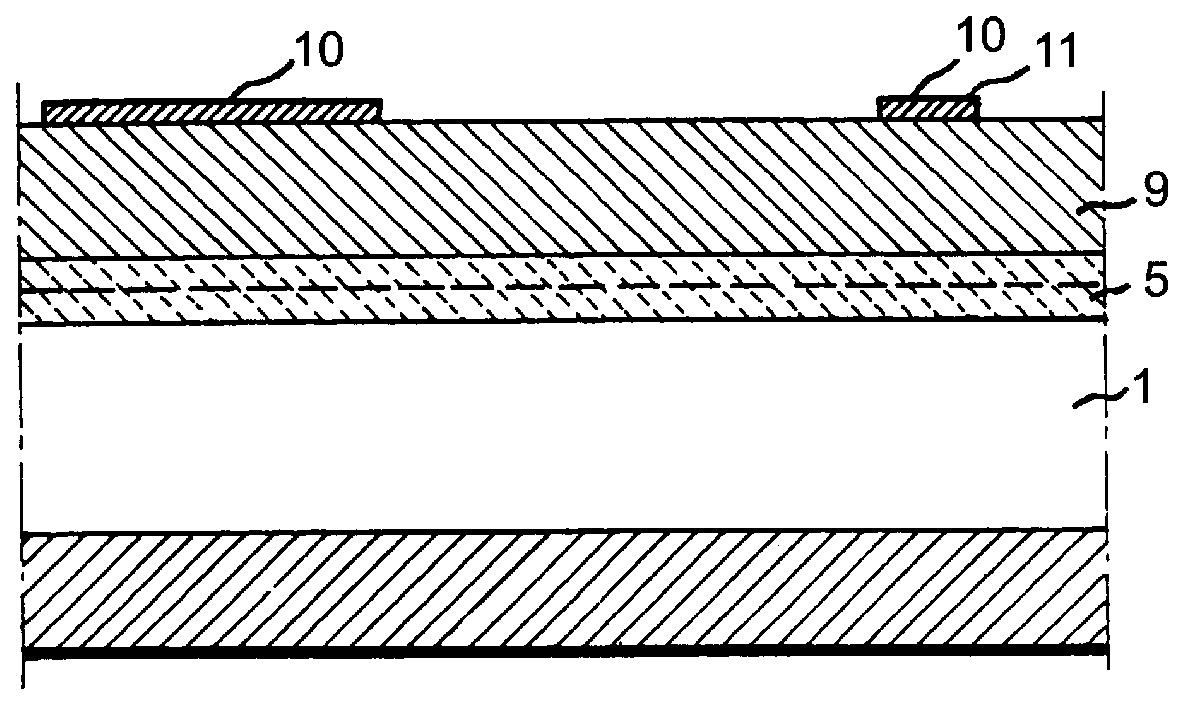
FIGS. 1-4 illustrate a few important steps of a larger number of steps in a method for producing the anode side of a power pin-diode of SiC. It should also be noticed that the present invention is only occupied with a method for producing a pn-junction for a semiconductor device of SiC and not to a method for producing the entire device, and a method of the type last mentioned comprises of course many more process steps, which will not be dealt with here.

An intrinsic or low doped n-type drift layer is epitaxially grown on top of a highly doped n-type substrate layer 2, on the back-side of which a contact layer 3 with an ohmic contact and a bond metallization is applied. The doping concentrations of the layers 1 and 2 are preferably in the ranges 10.sup.14 -10.sup.16 cm.sup.-3 and 10.sup.19 -5.times.10.sup.20 cm.sup.-3, respectively, and the donors used are preferably N or P.

The drift layer 1 extends to the line 4 before the method according to the invention is started. The method ac...


PUM


Abstract

A method for producing a pn-junction for a semiconductor device of SiC intended to have at least one lateral zone of junction termination with a lower doping concentration of a first conductivity type than a main zone for smearing out the electrical field at said junction comprising at least the step of applying a first layer of SiC over the entire surface and on top of a second layer of SiC. A mask is applied on the first layer over a portion thereof where said main zone and an ohmic contact are to be formed. It is after that etched through the first layer to the second layer while leaving a main zone of said first layer and a contact layer thereof under said mask.

Description

TECHNICAL FIELD OF THE INVENTION AND PRIOR ARTThe present invention relates to a method for producing a pn-junction for a semiconductor device of SiC intended to have at least one lateral zone of junction termination with a lower doping concentration of a first conductivity type than a main zone to even out the electrical field at said junction, said method comprising at least the steps of:a) applying a first layer of SiC of said first conductivity type, p or n, on top of a second layer of a second conductivity type, opposite to the first type, said first layer either 1) having a first sub-layer closest to said second layer able to form a pn-junction with an acceptably high breakdown voltage and a second sub-layer on top thereof able to form an ohmic contact for the device, or 2) being one layer able to both form a pn-junction with an acceptably high break-down voltage and an ohmic contact for the device, wherein in case of 1) the sub-layers are applied in different steps,b) applyin...

Claims


Application Information

Patent Timeline
Patent Type & Authority Patents(United States)
IPC IPC(8): H01L21/04H01L29/66H01L21/02H01L29/861H01L29/02H01L29/24
CPCH01L21/046H01L29/6606H01L29/8613H01L29/0615H01L29/1608Y10S438/931
Inventor NILSSON, PER-.ANG.KE
Owner CREE INC
Why Eureka
Try Eureka