Contact test circuit

a test circuit and contact technology, applied in the direction of electric connection testing, measurement devices, instruments, etc., can solve the problems of limited device set, difficult to distinguish between the capacitance of i/o wiring and the capacitance of a fet gate, and the fet gate does not represent a practical impedance to use for contact verification

Inactive Publication Date: 2000-07-11
IBM CORP
View PDF7 Cites 27 Cited by
  • Summary
  • Abstract
  • Description
  • Claims
  • Application Information

AI Technical Summary

Problems solved by technology

There is a limited set of devices on the typical DUT that lend themselves to simple impedance analysis.
It would be difficult to distinguish between the capacitive impedance of a FET gate and the capacitance of I/O wiring.
Thus FET gates do not represent a practical impedance to use for contact verification.
The impedance at these I/O pads is so high that there is a considerable ri

Method used


Image

  • Contact test circuit
  • Contact test circuit
  • Contact test circuit

Examples


Embodiment Construction

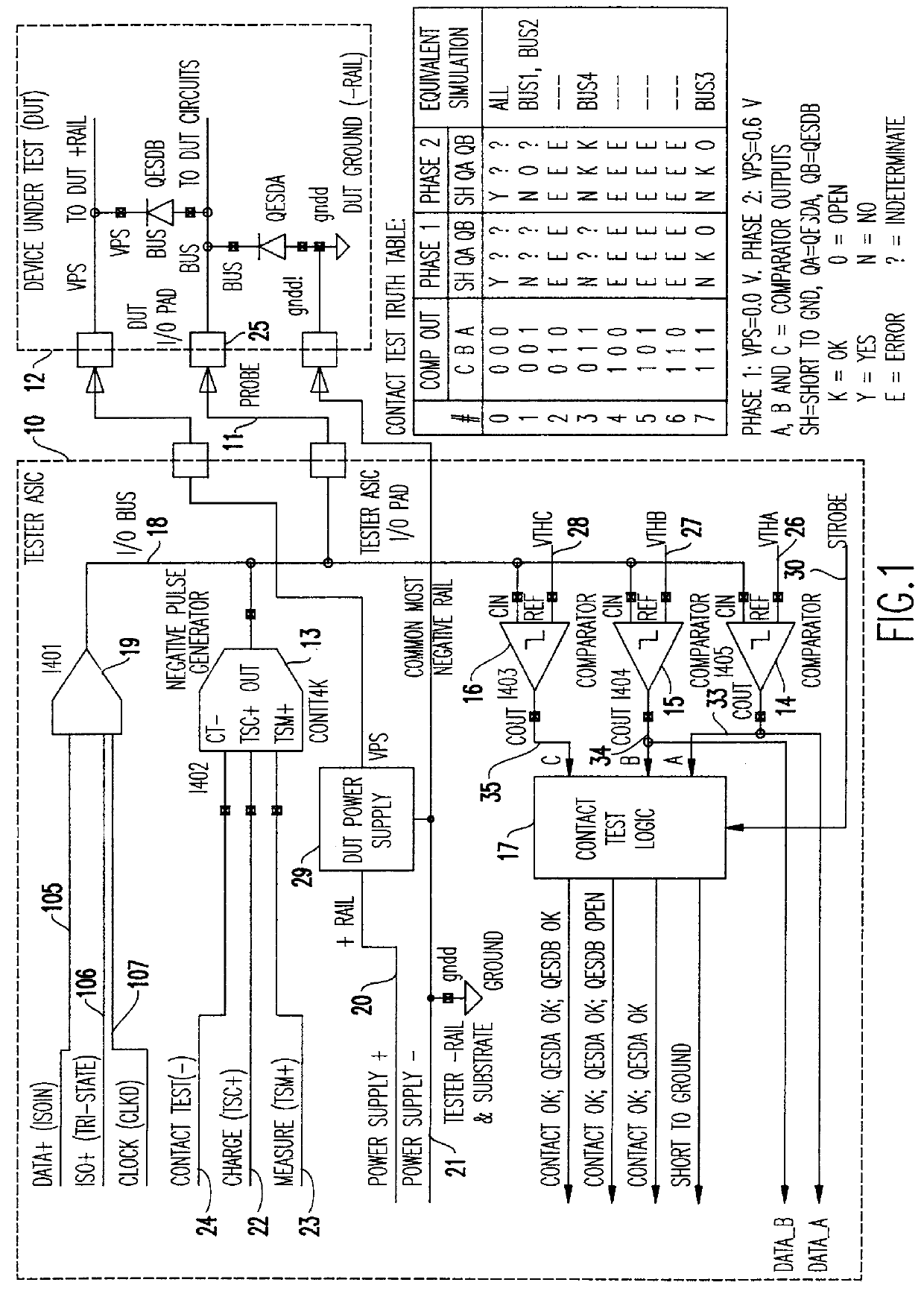
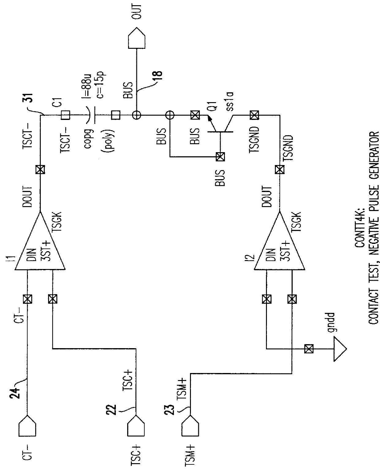
Referring now to the drawings, and more particularly to FIG. 1, there is shown a typical interface between a test device 10, a test probe 11, and a device under test (DUT) 12. Although only one probe connection 11 is shown, many more identical simultaneous connections may exist. Tester 10 is constructed in accordance with the invention, and in the best mode this circuitry is implemented in a single integrated circuit (ASIC) that includes a NEGATIVE PULSE GENERATOR 13 (designated as CONTT4K in the figures), COMPARATORS 14, 15 and 16, and CONTACT TEST LOGIC 17. The pulse generator 13 is used only for contact test. The pulse generator 13 assumes a high impedance state when contact test is ended so that it does not load the I / O Bus 18 during normal data transmission. The COMPARATORS 14, 15 and 16 may be used for contact test, but their main function is for sensing normal data on the I / O BUS 18. CONTACT TEST LOGIC 17 evaluates the results of contact test. The ISOLATING DATA DRIVER 19 ser...


PUM


Abstract

A method and apparatus for contact testing a plurality of devices under test, either sequentially or simultaneously. In a first test phase it is determined whether the test probe to each contact is shorted to the most negative rail. In a second phase it is determined whether the test probe has made proper contact, and whether ESD diodes on the devices under test are functional. In both test phases a negative pulse is generated on a tester bus and applied to the contact by the test probe. In the first test phase the positive rail of the device under test is grounded; in the second test phase the positive rail of the device under test is made positive. The negative rail of the device under test is connected to the negative rail of the tester. In both test phases, upon termination of the negative pulse, the bus is restored to a positive voltage which is dependent upon the condition of the contact and the condition of expected input devices at the contact. The bus voltage is measured in accordance with a logic which determines the condition of the contact and the condition of expected input devices at the contact. Data signals for functional testing of the device under test are can be applied to the bus through an isolating driver which preserves the logic of the contact test.

Description

1. Field of the InventionThe present invention generally relates to assuring that there is electrical contact between test probes and input / output pads of an integrated circuit device, prior to testing of the functional characteristics of the integrated circuit. More specifically, the invention relates to an apparatus and method for determining whether there is electrical contact between test probe and pad where the tester has no power supply more negative than the most negative power supply rail of the circuit being tested, and where the test current must flow through electrostatic discharge (ESD) diodes whose polarity requires that a contact test signal more negative than the most negative rail of the circuit under test be applied by the probe to the pad.2. Background DescriptionWhen a tester is to be used to test integrated circuits on a wafer, all tester probes must be aligned exactly with the wafer I / O pads to assure meaningful tests. A group of the I / O pads may be devoted to o...

Claims


Application Information

Patent Timeline
IPC IPC(8): G01R31/02G01R31/04
CPCG01R31/043G01R31/68
Inventor BONACCIO, ANTHONY R.LEIGHTON, HOWARD J.
Owner IBM CORP
Why Eureka
Try Eureka