Silicon-on-insulator and CMOS-on-SOI double film fabrication process with a coplanar silicon and isolation layer and adding a second silicon layer on one region

a technology of silicon-on-insulator and isolation layer, which is applied in the direction of semiconductor devices, electrical equipment, transistors, etc., can solve the problems of not being able to protect esd, and not being able to meet the requirements of esd protection,

Inactive Publication Date: 2000-08-01
GLOBALFOUNDRIES INC
View PDF14 Cites 111 Cited by
  • Summary
  • Abstract
  • Description
  • Claims
  • Application Information

AI Technical Summary

Problems solved by technology

SOI complimentary metal-oxide semiconductor (CMOS) output buffers do not perform as well as "bulk" CMOS output buffers formed in the silicon substrate for either positive or negative ESD impulses.
Given ESD structures are also designed in the silicon layer (e.g., they are made of diodes or SOI metal oxide field effect transistors (MOSFETs)), ESD protection, as a general rule, will not be as good as bulk devices where the heat can be dissipated to the bulk and where the film thickness is greater.
In SOI, certain ESD concepts will not work.
For example, thick field oxide ESD structures are impractical.
In thin film SOI, these structures are not constructable or available to form standard diodes, pnp transistors, npn

Method used


Image

  • Silicon-on-insulator and CMOS-on-SOI double film fabrication process with a coplanar silicon and isolation layer and adding a second silicon layer on one region
  • Silicon-on-insulator and CMOS-on-SOI double film fabrication process with a coplanar silicon and isolation layer and adding a second silicon layer on one region
  • Silicon-on-insulator and CMOS-on-SOI double film fabrication process with a coplanar silicon and isolation layer and adding a second silicon layer on one region

Examples


Embodiment Construction

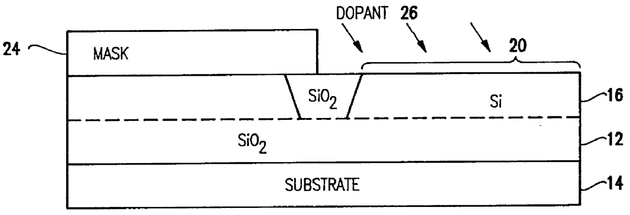
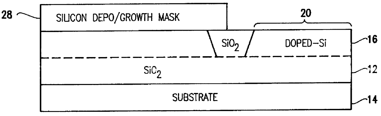
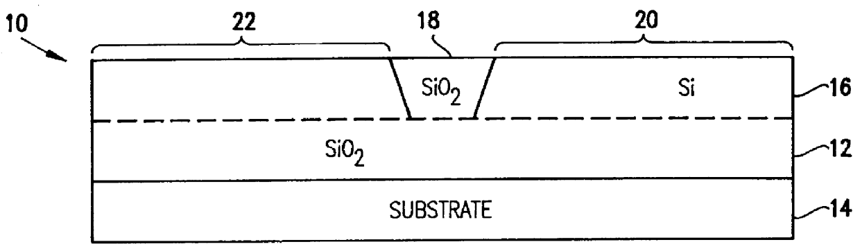
FIGS. 1a-h illustrate one embodiment of a fabrication process according to this invention. Starting with a substrate such as wafer 10 having a buried oxide layer 12 separating bulk substrate 14 and a surface silicon film 16, a dielectric isolation 18, such as a trench isolation or a MESA isolation, is formed on the buried oxide layer 12 to separate regions 20 and 22. The wafer 10 is representative of starting materials for SOI and SOS devices well known in the art, and the isolation structure 18 can be created by any of a number of wellknown techniques and serves the purpose of providing isolated structures 20 and 22 on the wafer 10. FIG. 1a shows only structures 20 and 22 for illustrative purposes, and it should be understood by those of skill in the art that the wafer 10 will have several isolated structures 20 and 22 on its surface, each being separated by dielectric isolation 18.

Well implants (N and P) are then completed as needed by the SOI or SOS device. FIG. 1b shows a patter...


PUM


Abstract

Silicon is formed at selected locations on a silicon-insulator (SOI) substrate during fabrication of selected electronic components, including resistors, capacitors, and diodes. The silicon location is defined using a patterned, removable mask, and the silicon may be applied by deposition or growth and may take the form of polysilicon or crystalline silicon. Electrostatic discharge (ESD) characteristics of the SOI device is significantly improved by having a thick double layer of silicon in selected regions.

Description

DESCRIPTION1. Field of the InventionThe present invention generally relates to silicon-on-insulator (SOI) semiconductor devices and, more particularly, to a structure and fabrication process which provides for more robust electrostatic discharge (ESD) protection in SOI devices.2. Background DescriptionSOI complimentary metal-oxide semiconductor (CMOS) output buffers do not perform as well as "bulk" CMOS output buffers formed in the silicon substrate for either positive or negative ESD impulses. Given ESD structures are also designed in the silicon layer (e.g., they are made of diodes or SOI metal oxide field effect transistors (MOSFETs)), ESD protection, as a general rule, will not be as good as bulk devices where the heat can be dissipated to the bulk and where the film thickness is greater. In practice, SOI output buffers have been shown to have two times lower ESD robustness when compared to bulk CMOS output buffers.In general, circuit elements which compose input / output (I / O) ci...

Claims


Application Information

Patent Timeline
IPC IPC(8): H01L21/70H01L27/12H01L21/84H01L27/02H01L27/04H01L21/822H01L29/786
CPCH01L21/84H01L27/0251H01L27/1203H01L21/18
Inventor ELLIS-MONAGHAN, JOHN J.VOLDMAN, STEVEN H.
Owner GLOBALFOUNDRIES INC
Why Eureka
Try Eureka