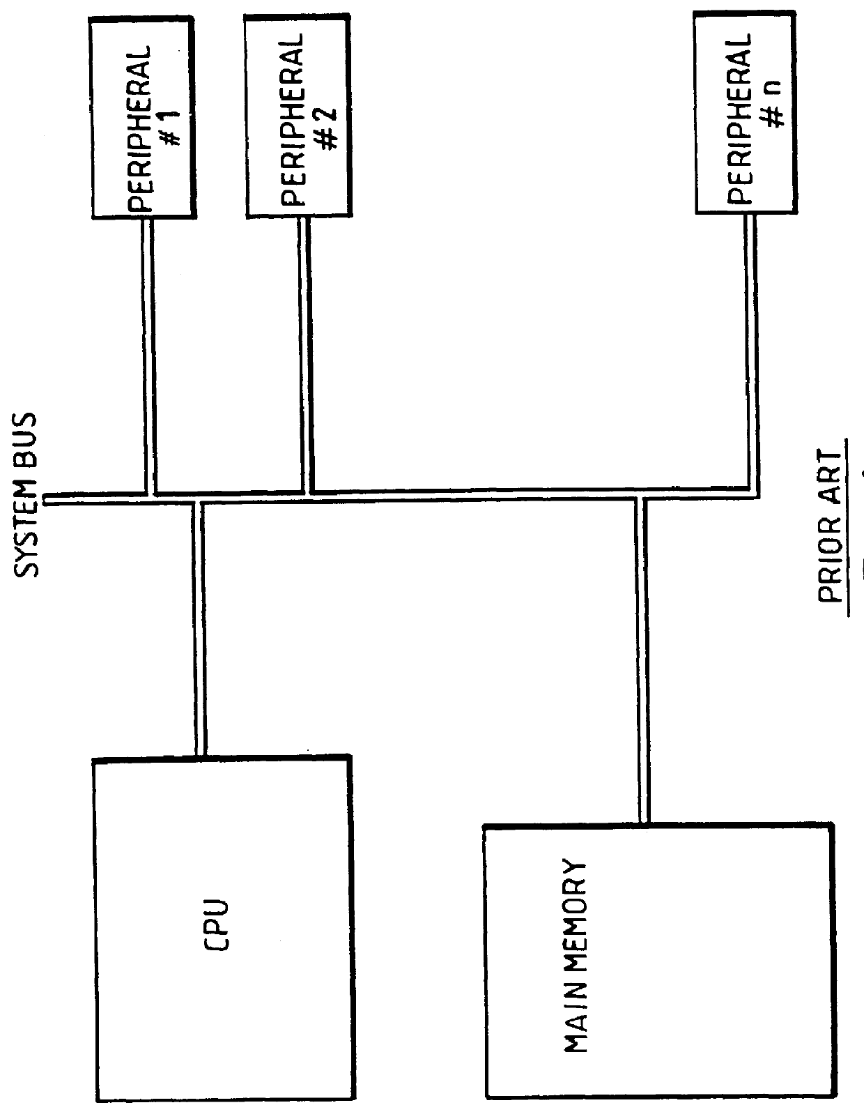
This is relatively straight forward design and provides room for expansion; but it has serious limitations.
Thus the amount of concurrent activity in the system is limited by the overall capacity of the external
bus.
Increasing the bus bandwidth, however, is much more difficult and very costly to the point of becoming technically impossible or prohibitively expensive.
In addition, the number of I / O resources which can be on the bus is also limited by the bandwidth.
It should be noted indeed that while theoretically the single bus allows a high order of expandability, the real operation due to contentions, drastically limits such expansion.
This problem is prevalent among all types of applications.
The large number of transfers and the time spent in arbitration consume a significant part of the available data bandwidth and also reduce the CPU
access frequency.
As the number of network interfaces increases or higher speed interfaces are added, the amount of time available to each resource, including CPU, decreases, thus clipping the peak performance of the system.
It also forces the designers to go for even higher performance CPUs and associated expensive components, thus driving up the cost.
The number of networks which can be connected via this prior art type of
system bus also remains low due to these severe limitations, and this problem becomes worse as more and more networks at higher and higher speeds are added to accommodate, for example,
the Internet related expansion activity, and is unscalable approach.
The first task requires a large number of frequent data transfers, called `BitBlt`, from one place in the memory to another; but this requirement tends to be bursty in nature.
This consumes a considerable portion of the system bandwidth and thus has necessitated the use of separate memory to store
graphics data, as shown in later-described FIG. 5, thereby adversely affecting the system cost.
This large number of transfers, moreover, is required in a short time, thus consuming most of the available data bandwidth in a small time slot, starving the CPU and other I / O resources.
Before the present invention, however, no practical breakthrough has been offered in this area by the existing DRAM manufacturers to alleviate this problem.
It is a significant requirement which is difficult to meet with the conventional DRAM, if also used as main memory.
This, therefore, led to the development of more expensive specialized DRAMs and one of the popular and extensively used such special DRAM is `Video DRAM` also called `VRAM`.
They are, however, more expensive than traditional DRAMs due to the larger number of additional pins and the bigger
silicon die, and the architecture provides a very
rigid structure.
Expandability to more interfaces with more devices is severely limited as the number of pins grows significantly.
This approach requires CPU intervention, limiting the switching speed and also does not solve the problem of speeding the huge data movement requirements.
VRAMs (specifically the 3 port version) were also occasionally touted towards networking applications but have rarely been so used due to their before-stated rigid I / O structure, very limited capability to interconnect number of resources (to be precise--only two) and to
handle both large and small packets efficiently, bigger board space, more expensive construction and
higher power consumption.
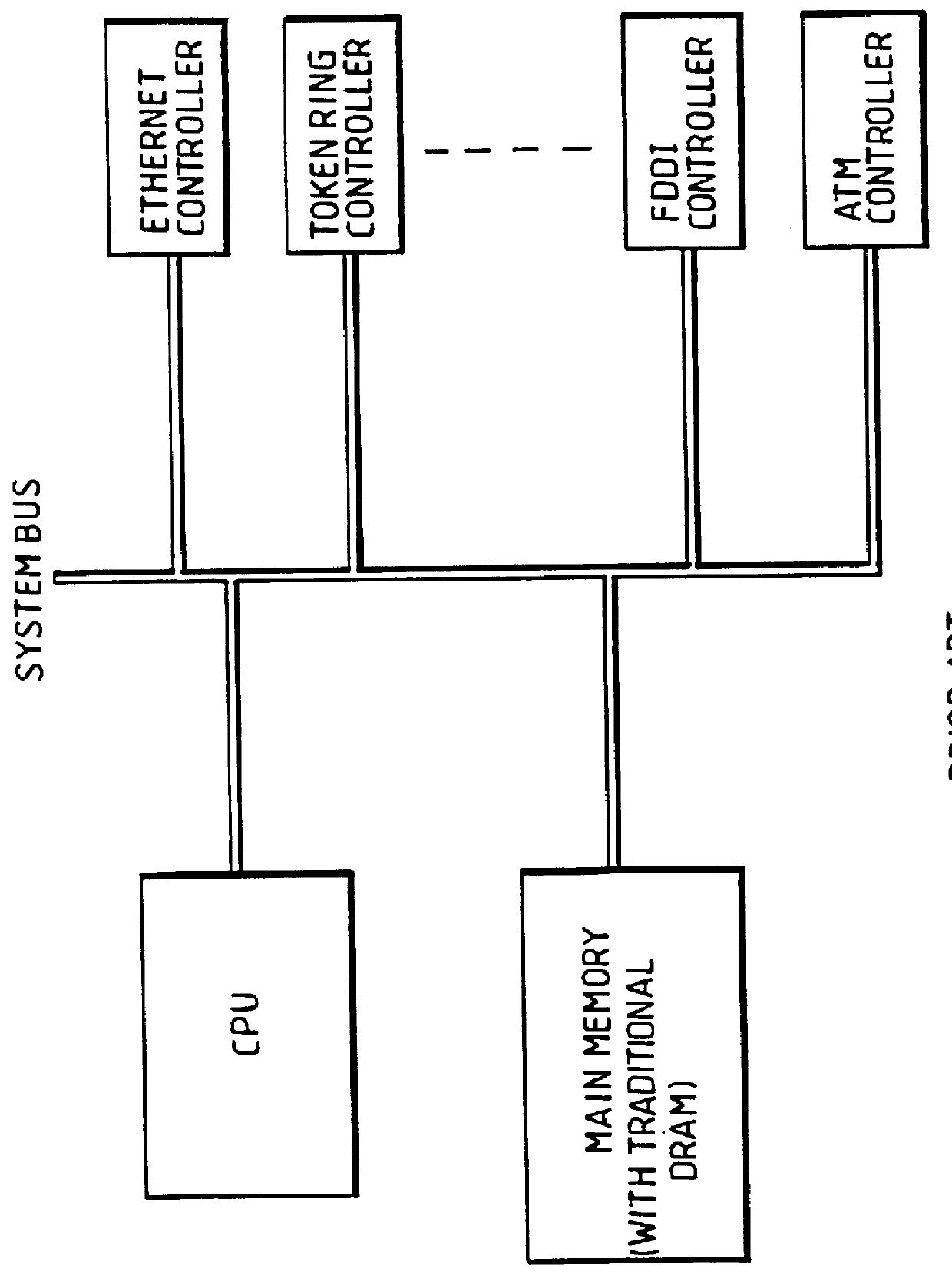
In summary, therefore, the typical prior art and current system configurations based on traditional DRAMs (such as before-mentioned FIG. 3) are burdened with the limitations described above.
The problems associated with the networking applications, where a large number of high speed networks need be interconnected at low cost, have remained largely unsolved, thus resulting in higher price per network interfaces.
While the system bandwidth limitations and the constant
CRT display update requirements led to the development of video DRAMs, primarily intended for
graphics applications and generally used in configurations such as shown in FIG. 6, as previously discussed, and while this configuration performs better than compared to the traditional DRAMs, as performance requirements on both the main memory and the display data bandwidth increased, the deleterious
side effect of this configuration added cost to the system due to separation of main memory from graphics memory and also due to the higher cost of the VRAMs themselves.
One possibility is to use VRAMs as both the graphics and the main memory components; but the added cost of the components neutralizes the gains achieved by having a common memory.
But unfortunately because of their block-oriented protocol and interface limitations, it is highly inefficient with non-localized main memory accesses, and thus does not render itself well to the concept of `Unified
Memory Architecture`.
Use of RDRAM also poses a host of significant electrical
engineering design challenges related to the emissions,
noise interference and PCB
layout, making the design task very difficult.

