Method for making DRAM capacitor strap

a technology of dram capacitors and straps, which is applied in the direction of semiconductor devices, electrical apparatus, transistors, etc., can solve the problems of increased chance of error or contamination, increased cost of producing such a structure, and excessive defect rate of conventional processes

Inactive Publication Date: 2000-08-29
INFINEON TECH AG +1
View PDF13 Cites 28 Cited by
  • Summary
  • Abstract
  • Description
  • Claims
  • Application Information

AI Technical Summary

Problems solved by technology

One of the challenges associated with trench DRAM processing is the formation of an electrical connection between the trench capacitor and the diffusion region of the array device pass transistor.
This increases the cost of producing such a structure.
Further, because of the multiplicity of steps required, the chance for error or contamination increases with each additional processing step.
Therefore, the defect rate of the conventional process is excessive.

Method used


Image

  • Method for making DRAM capacitor strap
  • Method for making DRAM capacitor strap
  • Method for making DRAM capacitor strap

Examples


Embodiment Construction

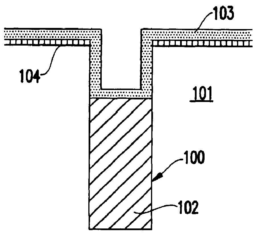
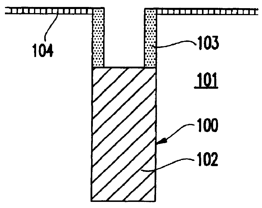
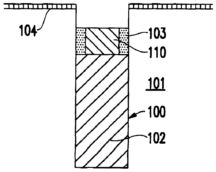
Referring now to the drawings, and more particularly to FIG. 2A, a trench 200, formed in a substrate 201 is illustrated. The substrate, 201, is preferably a silicon substrate. The trench 200 is a deep trench capacitor in this example. However, the invention is not limited to deep trenches capacitor, but could include any type of similar trench.

As discussed above, the trench 200 can initially be lined with a dielectric insulating layer. Then, the trench is partially filled with a first layer of conductive material 202 which is preferably polysilicon, but could also comprise metal or any other conductive material and a pad nitride 204, such as silicon nitride, is formed. As is known by one ordinarily skilled in the art, the trench 200 is formed by conventional processes including lithography, mask etching, mask removal, wet cleaning. Similarly, the formation of the first layer of conductive material 202 can include low-pressure chemical vapor deposition (LPCVD) dry polysilicon etching...


PUM


Abstract

A method of forming a trench capacitor comprises steps of forming a trench in a substrate, partially filling the trench with a first conductive material, lining a portion of the trench above the first conductive material with a collar material, etching the collar material to a strap depth below a top of the trench, and filling the trench with a second conductive material, wherein a portion of the second conductive material positioned between the strap depth and the top of the trench comprises a buried strap.

Description

1. Field of the InventionThe present invention generally relates to the formation of an electrical connection between trench capacitors and semiconductor transistors and more specifically to an improved method of forming a buried strap to make such an electrical connection.2. Description of the Related ArtTrench storage cells are used in dynamic random access memory (DRAM) products due to the high degree of planarity obtainable with the trench structure during chip processing. One of the challenges associated with trench DRAM processing is the formation of an electrical connection between the trench capacitor and the diffusion region of the array device pass transistor.Conventionally, as shown in FIG. 1F, a "buried strap" 120 connection is made between the top of the trench 100 and the diffusion region (i.e., drain 134) of the transistor 130. The buried strap 120 connection eliminates the requirement for a distinct lithographic patterning level. However, multiple polysilicon deposit...

Claims


Application Information

Patent Timeline
Patent Type & Authority Patents(United States)
IPC IPC(8): H01L21/70H01L21/8242H01L27/108H01L27/10
CPCH01L27/10861H10B12/038H01L27/10
Inventor BRONNER, GARY B.RADENS, CARL J.WITTMANN, JUERGEN
Owner INFINEON TECH AG
Why Eureka
Try Eureka