Optoelectronic device with separately controllable carrier injection means

a technology of optoelectronic devices and carrier injection means, which is applied in the direction of solid-state devices, basic electric elements, electric devices, etc., can solve the problems of not being operationally compatible with signal processing circuitry, not being able to monolithically integrate with the existing silicon integrated circuit technology, and high cost of devices, so as to reduce the avalanche breakdown voltage of devices, increase surface area, and reduce the distance between the first junction region

Inactive Publication Date: 2000-08-29
PRETORIA UNIV OF
View PDF7 Cites 70 Cited by
  • Summary
  • Abstract
  • Description
  • Claims
  • Application Information

AI Technical Summary

Benefits of technology

The said highly doped region may be imbedded in a base layer of the same, but higher doping concentration as the epitaxial layer, to reduce the avalanche breakdown voltage of the device.
In another embodiment the said highly doped region may be in the form or shape of a grid embedded in the epitaxial layer so that the first junction region periodically extends up to the surface region of the device, thereby to increase the surface area of the first junction region and to decrease the distance between the first junction region and the surface region.
The gates may be resistive gates, extending radially outwardly, so that voltage profiles may be generated in a radial direction in the gates, thereby to facilitate control of uniformity of light emission and the spatial location of the light emission region.
Typical applications of the device include on chip displays, electro-optical coupling interfaces to and from external components, internal electro-optical coupling where a device according to the invention on a chip may act as a light emitting device and another similar device on the same chip may act as a photo-detector. In this case the aforementioned guard ring structure preferably defines suitably positioned windows. The windows or interruptions in the guard rings cause breakdown in these regions rather than along a bottom plane of the junction, to enable light to propagate, laterally in the chip. The highly doped region may be made to extend deeper into the epitaxial layer for better lateral emission,
The invention also provides an optoelectronic device comprising a first layer of a suitable material adjacent a second layer of a doped indirect bandgap semiconductor material, to provide a first junction region at a metallurgical interface between said first layer and said second layer, the first junction region, in use, being reverse biased to beyond avalanche breakdown to cause the device to act as a light emitting device, the light emission being caused by a reverse current drifting across said first junction region, the device further comprising means for providing additional carriers in said first junction region, thereby to enhance the emission of light by the device.

Problems solved by technology

These devices are expensive, are not operationally compatible with the signal processing circuitry found on silicon integrated circuits and cannot monolithically be integrated with the existing silicon integrated circuit technology.

Method used


Image

  • Optoelectronic device with separately controllable carrier injection means
  • Optoelectronic device with separately controllable carrier injection means
  • Optoelectronic device with separately controllable carrier injection means

Examples


third embodiment

In FIG. 9 there is shown the device according to the invention designated 30. Also in this case the substrate 31, metal voltage / current feed layers 33, field oxide layers 35 and glass passivation layers 37 are well known in the art.

The heavily doped n.sup.+ region 32 of this device is in the form of a grid 34. Accordingly, the surface area of the n.sup.+ p junction region 36 has been increased compared to that of the embodiments hereinbefore described. Furthermore, the distance from the n.sup.+ p junction 36 to the surface 38 of the device has been reduced, resulting in less optical absorption in the near surface regions and thus increased emission of generated light.

The n.sup.+ region 32 is embedded in a higher doped p ion implanted base layer 40 than the p.sup.- epilayer 44 in order to reduce the avalanche breakdown voltage voltage and thus to induce light emission at a lower operating voltage.

The n-well guard rings 42 prevent light emission from the lateral peripheral regions of ...

fourth embodiment

In FIG. 10 there is shown the device according to the invention designated 50. Also in this case the structure and function of the substrate 51, metal voltage / current feed layers 53, field oxide passivation layers 55 and glass passivation layers 57 are well known in the art.

The n.sup.+ region 52 of this device comprises a plurality of radially spaced concentric rings 54.1, 54.2 and 54.3. At the origin of the circle there is provided a p.sup.+ region 56. The rings 54.1 to 54.3 and p.sup.+ region 56 are embedded in a p-base region 58, to lower the avalanche breakdown voltage and accordingly the operating voltage of the device. The rings 54.1 to 54.3 are inter-connected by n.sup.+ regions (not shown) causing a potential gradient from the inner to outer n.sup.+ concentric rings when breakdown has occurred. The p-base region is embedded in a p.sup.- epitaxial layer.

The placement of the n.sup.+ and p.sup.+ regions designated 52 and 56 respectively and the geometrical layout of these regio...

fifth embodiment

In FIGS. 11 and 12 there is shown the device according to the invention and which is designated 60.

The device is similar to the fourth embodiment shown in FIG. 10, but further comprises a controllable circular conductive gate 64 between the centre p.sup.+ region 62 and the concentric n.sup.+ circles 66. The gate is located on an oxide layer 61.

Referring firstly to FIG. 11, with the n.sup.+ and p.sup.+ regions (designated 66 and 62 respectively) reverse biased via terminals 70 and 68, and with a positive voltage applied to terminal 72, majority carriers from the substrate 74 are attracted towards the surface 76, to increase the doping level of the surface region between the n.sup.+ and p.sup.+ regions. This results in a lowering of the avalanche breakdown voltage. Since the gate electrodes 64 induce surface inversion, depletion or accumulation only and draw no current, they may be used as controlling terminals for switching on the light emission between the n.sup.+ and p.sup.+ region...


PUM


Abstract

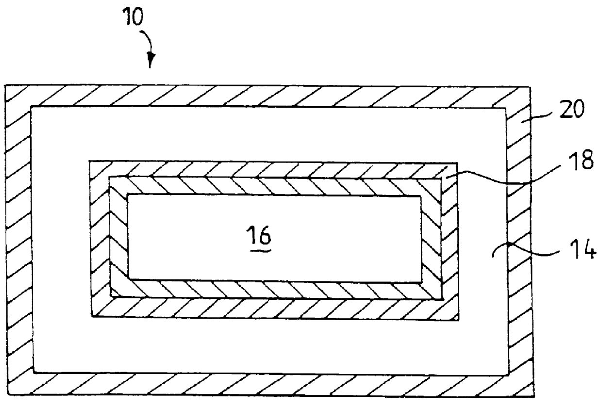
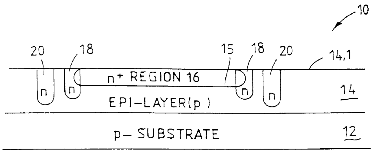
An optoelectronic device (10) formed in a chip of an indirect bandgap semiconductor material such as silicon is disclosed and claimed. The device comprises a visibly exposed highly doped n+ region (16) embedded at the surface of an oppositely doped epitaxial layer (14), to form a first junction region (15) closed to the surface of the epitaxial layer. When the junction region is reverse biased to beyond avalanche breakdown, the device acts as a light emitting device to the external environment. When it is reversed biased to just below avalanche breakdown it acts as a light detector. The device may further include a further junction region for generating or providing additional carriers in the first junction region, thereby to improve the performance of the device. This further junction can be multiplied to facilitate multi-input processing functions where the light emission from the first junction is a function of the electrical signals applied to the further junctions.

Description

INTRODUCTION AND BACKGROUNDTHIS invention related to indirect bandgap semiconductor technology (such as silicon integrated circuit technology) and more particularly to discrete and monolithically integrated opto-electronic devices produced from these semiconductor materials.The present known solid state light emitting devices comprise complex structures of composite direct bandgap semiconductor materials from the Group II, III, V and VI elements, for example galium-arsenide-phosphide. These devices are expensive, are not operationally compatible with the signal processing circuitry found on silicon integrated circuits and cannot monolithically be integrated with the existing silicon integrated circuit technology.OBJECT OF THE INVENTIONIt is an object of the present invention to provide an optoelectronic device and a method of producing same with which the applicant believes the aforementioned disadvantages may at least be alleviated.According to the invention there is provided an op...

Claims


Application Information

Patent Timeline
Patent Type & Authority Patents(United States)
IPC IPC(8): H01L33/00H01L33/34
CPCH01L33/0008H01L33/34
Inventor SNYMAN, LUKAS W.AHARONI, HERZLDUPLESSIS, MONUKO
Owner PRETORIA UNIV OF
Why Eureka
Try Eureka