
Clamping circuit and method for synchronous rectification

a synchronous rectifier and clamping circuit technology, applied in the direction of electric variable regulation, process and machine control, instruments, etc., can solve the problems of large voltage spikes and high frequency ringing typically generated in the rectifier, increase power loss so as to reduce peak voltage and dampen oscillation, suppress high voltage spikes, and dissipate a noticeable amount of power

Inactive Publication Date: 2000-10-03
ERICSSON INC
View PDF10 Cites 47 Cited by
  • Summary
  • Abstract
  • Description
  • Claims
  • Application Information

AI Technical Summary

Benefits of technology

Large voltage spikes and high frequency ringing are typically generated within a rectifier during fast switching transitions, primarily due to the presence of parasitic inductances in the transformer and parasitic capacitances in the transistor switches. As a result, higher rated devices are needed to prevent breakdown of the diodes and / or transistor switches. Because use of the higher rated devices increases the power loss, such use to suitably handle the excessive voltage spikes and high frequency ringing conflicts with the need for employing diodes and transistor switches to suitably maintain low power loss.
According to a first embodiment of the present invention, there is provided a rectifier circuit which reduces voltage spikes and high frequency ringing caused by parasitic components therein. The rectifier circuit is a synchronous rectifier having at least two transistor switches connected to the secondary side of a transformer. The transistor switches are selectively switched between conductive and non-conductive states by control signals generated from the primary side and secondary side of the isolation transformer via a control circuit. The present invention includes a first voltage clamping component having a first terminal which is connected to a first end of the secondary side of the transformer, and a second voltage clamping component having a first terminal which is connected to a second end of the secondary side of the transformer. The present invention further includes a third component connected to a second terminal of the first and second voltage clamping components. The third component additionally drives the control circuit.

Problems solved by technology

Large voltage spikes and high frequency ringing are typically generated within a rectifier during fast switching transitions, primarily due to the presence of parasitic inductances in the transformer and parasitic capacitances in the transistor switches.
Because use of the higher rated devices increases the power loss, such use to suitably handle the excessive voltage spikes and high frequency ringing conflicts with the need for employing diodes and transistor switches to suitably maintain low power loss.
However, the snubber circuits (FIG. 1) dissipate a noticeable amount of power and peak voltages within the rectifier nonetheless remain.
The active clamping circuits, however, substantially increase the complexity and component count of the rectifier.
When either of the transistor switches is switched into the non-conductive state, a relatively large voltage spike and high frequency ringing are induced thereat due to a parasitic inductance and capacitance in the transformer and transistor switch, respectively.

Method used


Image

  • Clamping circuit and method for synchronous rectification
  • Clamping circuit and method for synchronous rectification
  • Clamping circuit and method for synchronous rectification

Examples


Embodiment Construction

The present invention will now be described more fully hereinafter with reference to the accompanying drawings in which preferred embodiments of the invention are shown. This invention may, however, be embodied in many different forms and should not be construed as being limited to the embodiments set forth herein. Rather, the embodiments are is provided so that this disclosure will be thorough and complete, and will fully convey the scope of the invention to those skilled in the art.

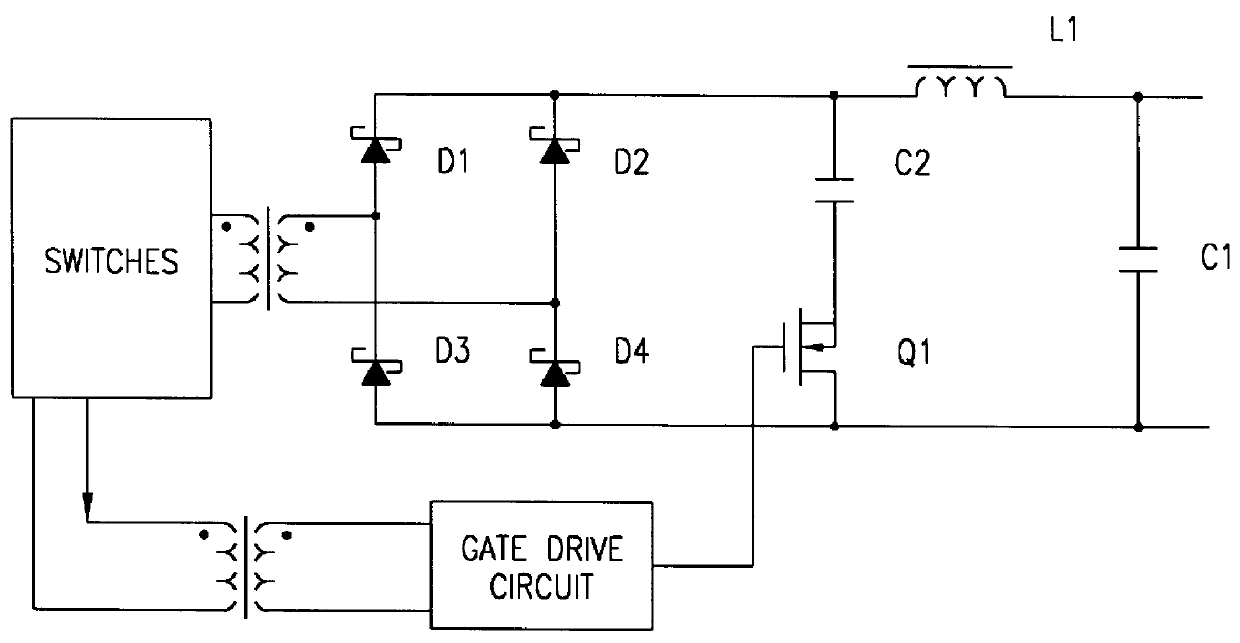
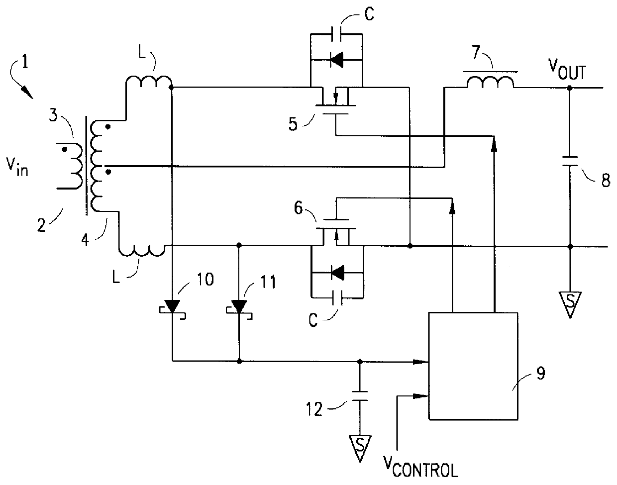
Referring to FIG. 3, there is shown a rectifier circuit 1 according to a preferred embodiment of the present invention as part of a power supply. Rectified circuit 1 of FIG. 3 is a full wave synchronous rectifier circuit including transformer 2 having primary side or winding 3 and secondary side or winding 4, and transistor switch 5 having a first terminal connected to a first end of secondary winding 4 and a second terminal connected to a ground reference. Rectifier circuit 1 further includes a second ...


PUM


Abstract

A rectifier circuit having voltage clamping circuitry is disclosed. The rectifier circuit includes a transformer having a primary winding and a secondary winding and transistor switches each being connected to an end of the secondary winding of the transformer. The rectifier circuit further includes a first diode having an anode terminal connected to a first end of the secondary winding and a second diode having an anode terminal connected to a second end of the secondary winding. The cathode terminals of the first and second diodes are coupled to a capacitor. The energy stemming from voltage spikes and / or high frequency ringing appearing at the transistor switches due to parasitic effects is effectively absorbed by the first and second diodes and collected in the capacitor. The collected energy is recycled to control the operation of the transistor switches.

Description

1. Technical Field of the InventionThe present invention relates to a power converter, and particularly to a synchronous rectifier having voltage limiting circuitry.2. Background and Objects of the InventionPower converters are known to convert an input voltage waveform having a DC component into a DC voltage waveform. Power converters employing an isolation transformer require employment of a rectification circuit to perform waveform conversion. Traditionally, rectifier circuits utilize diodes connected to the secondary side of the isolation transformer which conduct current only when forward biased. Synchronous rectifiers instead utilize transistor switches which are selectively turned on and off in synchronicity with the signal to be rectified in order to control conduction of current from the isolation transformer to the rectifier output.The advancement in computational speeds and densities of integrated circuitry and corresponding systems has led to a reduction in the operating...

Claims


Application Information

Patent Timeline
IPC IPC(8): H02M3/24H02M3/335H02M3/28H02M7/21H02M7/06H02M7/12
CPCH02M3/33592Y02B70/1475Y02B70/10H02M3/28
Inventor SUN, MARK N.HART, WILLIAM
Owner ERICSSON INC
Learn More