Low voltage, high speed multiplexer

a high-speed, low-voltage technology, applied in the field of circuitry, can solve the problems of insufficient potential to turn on either of the drivers, the less efficient operation of the ecl multiplexer illustrated in fig. 1 and the noise of transient signals, and achieve the effect of maximizing propagation speed, low stacking requirements, and fast output of selected signals

Inactive Publication Date: 2000-10-24
SEMICON COMPONENTS IND LLC
View PDF16 Cites 16 Cited by
  • Summary
  • Abstract
  • Description
  • Claims
  • Application Information

AI Technical Summary

Benefits of technology

In summary, the present invention is a multiplexer that provides for each input signal pair a pseudo-high-potential rail coupled to the high-potential nodes of a common-low-potential-node differential amplifier. The particular pseudo-rail that is selected provides a potential at the high-potential nodes of the differential amplifier that is higher than that provided at all other deselected differential amplifiers of the multiplexer. The output drivers coupled to the selected differential amplifier are thereby turned on, while the output drivers coupled to deselected amplifiers are not sufficiently forward-biased to turn them on. The preferential use of bipolar transistors rather than MOS transistors in the signal path aids in maximizing propagation speed. Another advantage of the present invention is the use of fewer active elements than are used in the prior-art design, thereby aiding propagation speed. The result is faster output of the selected signal than was available in the prior art. It is to be noted that the configuration of the multiplexer of the present invention may be implemented using MOS, bipolar, and BiCMOS transistor circuitry. The present invention further provides for low stacking requirements, which in turn makes low-voltage operation possible. The present invention is simpler than the prior-art multiplexer in that it reduces the number of active components previously used to perform the same function. This makes fabrication easier and causes a reduction in signal transmission delay, thereby making the circuitry faster than the prior art. Finally, noise improvement may be possible under certain operating conditions in that the output drivers are always biased to a non-zero potential; that is, near the operating point.

Problems solved by technology

The required charging up of the capacitance associated with the transistors of that stage of the circuit could lead to undesirable transient signal noise.
The ECL multiplexer illustrated in FIG. 1 is less efficient in operation than is desirable and possible.
Because of the potential drop associated with each resistance element there is insufficient potential to turn on either of those drivers.
However, that combination of drops is only just enough to keep those drivers off.
The output drivers coupled to the selected differential amplifier are thereby turned on, while the output drivers coupled to deselected amplifiers are not sufficiently forward-biased to turn them on.

Method used


Image

  • Low voltage, high speed multiplexer
  • Low voltage, high speed multiplexer
  • Low voltage, high speed multiplexer

Examples


Embodiment Construction

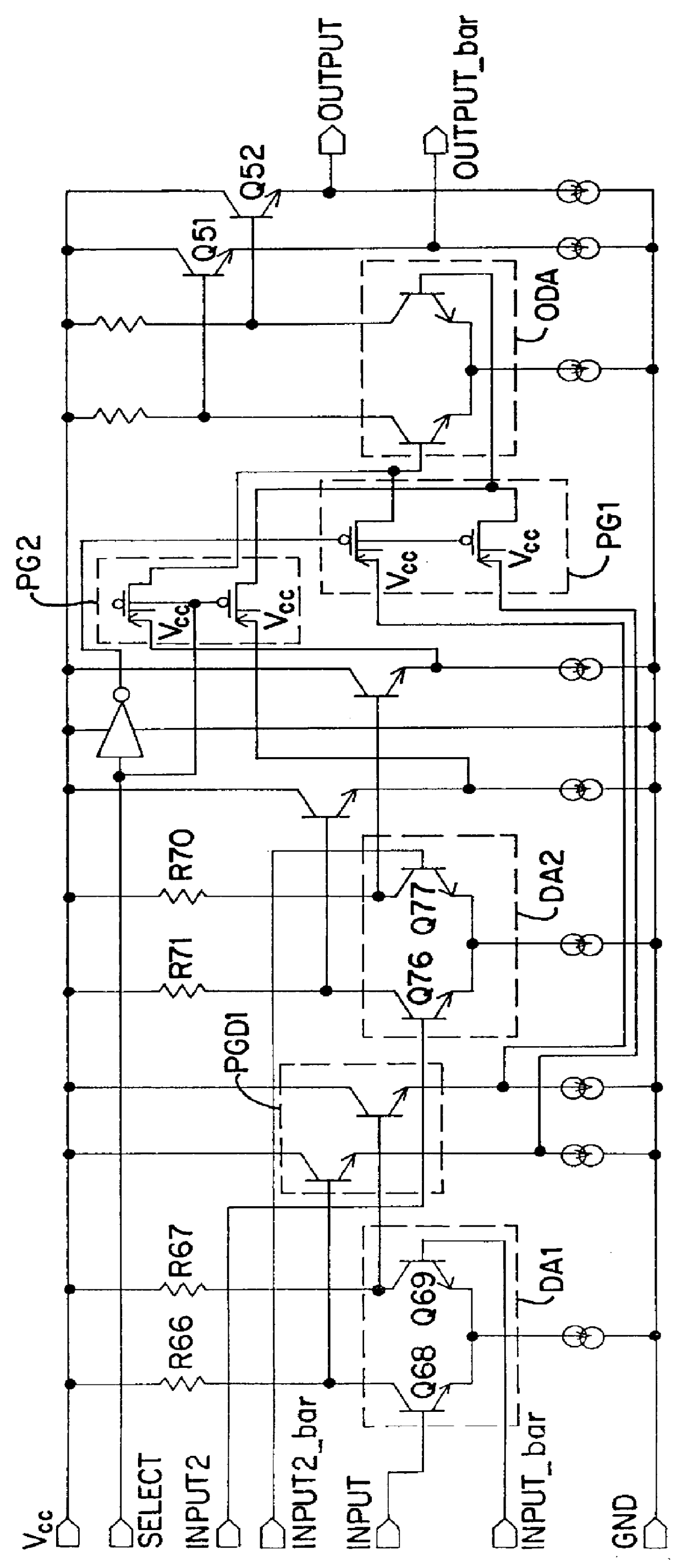
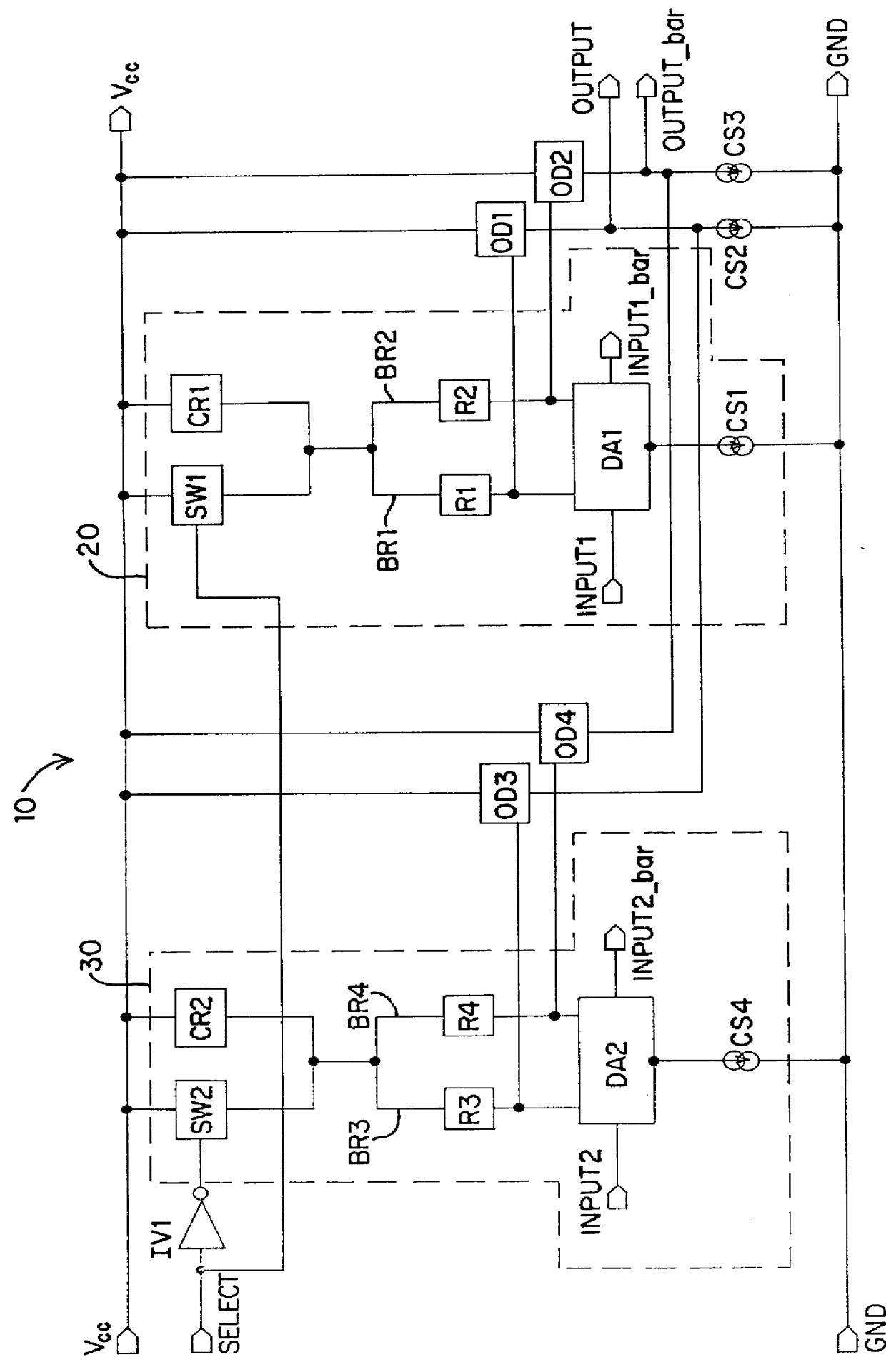
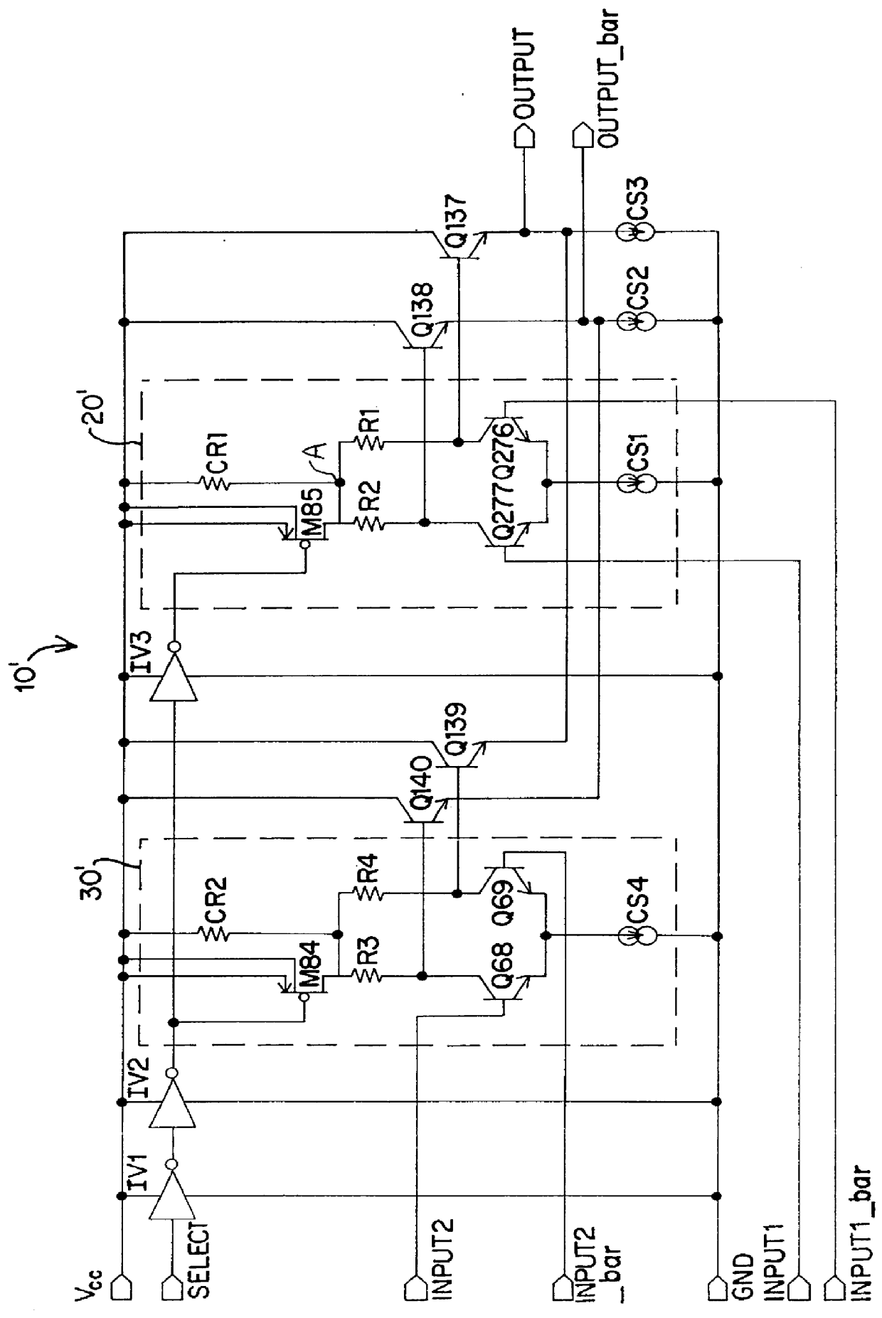
A multiplexer 10 of the present invention is shown in simplified form in FIG.2. The multiplexer 10 includes a plurality of control sub-circuits corresponding in number to the number of pairs of input signal pairs to be selected by the multiplexer 10 for output at the complementary output nodes output and output.sub.-- bar. For illustrative purposes, only two control sub-circuits, identified as sub-circuits 20 and 30, are shown in FIG. 2. However, it is to be understood that many more control sub-circuits may be employed as part of the multiplexer 10.

Control sub-circuit 20 includes a switch SW1, a common impedance element that is designated as a common resistance element CR1, a first resistance branch BR1 having first resistance element R1, a second resistance branch BR2 having second resistance element R2, and a differential amplifier DA1. Switch SW1 and common resistance element CR1 are each coupled directly to high-potential power rail Vcc. Switch SW1 may be any active element, su...


PUM


Abstract

A multiplexer for selecting a single output signal from a plurality of input signals. For a plurality of complementary input signal pairs in particular, the multiplexer includes for each pair of complementary input signals a control sub-circuit having a selection switch and a common resistance in parallel. The switch and the common resistance have a common low-potential node that is tied to a pair of resistances that are in parallel, wherein each of the parallel resistances is coupled to the respective high-potential nodes of a differential amplifier. A particular pair of incoming complementary input signal pairs controls the differential amplifier. An off-circuit selection signal selects which switch of a plurality of control sub-circuits is activated. When a switch is on, it creates a bypassing of the common resistance, thereby enabling the turn-on of output drivers coupled to the differential amplifier. When a switch is off, the potential drops across the common resistance and the parallel resistances reduce the potential at the output drivers' control nodes enough to block their turn-on. As a result, the only output drivers providing signal output are those associated with the one selected control sub-circuit having its switch turned on.

Description

1. Field of the InventionThe present invention relates to circuitry to aid in the routing of electrical signals from one location to another, such as from one semiconductor-based device to another. In particular, the present invention relates to the selection of particular electrical signals for transfer. More particularly, the present invention relates to multiplexers for selection / de-selection of electrical signals to be routed, including, but not limited to, emitter-coupled logic (ECL) signals.2. Description of the Prior ArtCircuits designed to aid in the selection of one or more electrical signals for routing from one device to another are commonly referred to as multiplexer circuits. Multiplexing circuits generally include a plurality of gating mechanisms that permit one and only one signal from a plurality of incoming signals to pass through from one device to another. Those devices may be on the same chip (as in the case of a microprocessor) or on different chips (such as bet...

Claims


Application Information

Patent Timeline
Patent Type & Authority Patents(United States)
IPC IPC(8): H03K17/62H03K17/693
CPCH03K17/6257H03K17/693
Inventor GOODELL, TRENOR F.FREITAS, OSCAR W.
Owner SEMICON COMPONENTS IND LLC
Why Eureka
Try Eureka