Multi-layer ceramic substrate and method for producing the same

a ceramic substrate and multi-layer technology, applied in the direction of sustainable manufacturing/processing, final product manufacturing, printed circuit non-printed electric components association, etc., can solve the problems of insufficient precision of printing paste, large variation in capacitance or other characteristics, and large variation in thickness of paste on the sh

Inactive Publication Date: 2000-11-28
MURATA MFG CO LTD
View PDF15 Cites 168 Cited by
  • Summary
  • Abstract
  • Description
  • Claims
  • Application Information

AI Technical Summary

Problems solved by technology

(1) Because variation in thickness of paste on the sheet is rather large and precision of printing the paste is insufficient, variation in capacitance or other characteristics is rather large.
(2) The paste on the green sheet is deformed in processes of pressure-joining the sheets and firing, which may cause variation in capacitance and like characteristics.
(3) Repeated printing and lamination of the sheets leads to deteriorated surface flatness of the printed portion, making it difficult to increase the number of sheets of the laminate or, in the case of a capacitor, to increase capacitance thereof.
This process may overcome the drawbacks involved in the first method; however, shrinkage behavior must be strictly controlled in the X, Y, and Z directions of ceramic green sheets, and the method has another drawback in that the materials which can be used as ceramic green sheets for providing substrates are considerably limited.
(1) When chip-type passive components are included within the space formed in a substrate, undesired gaps tend to be formed between the passive components and the corresponding inner surfaces extending perpendicular to the lamination planes, which gaps may cause formation of depressions at the surface of a substrate. Particularly, when the substrate is made of a glass-containing material, depressions become more significant, and in the worst case, cracks extending perpendicular to the lamination planes may be generated in the surface of the substrate or in the interface between the passive components and the substrate.
(2) The flatness of the substrate tends to deteriorate.
(3) Attaining a high dimensional precision is difficult.
(4) Formation of minute wiring is difficult.
However, these methods are not drawn to the case in which passive components are contained interior of a substrate.
As a result, the dielectric layer is exposed in an edge face of the substrate, and thus, the dielectric layer must be dense enough not to permit penetration of moisture.
(1) Low level of freedom in design, due to laminar placement of the dielectric in a substrate, and
(2) Problems such as crosstalk of signals tend to occur.
Moreover, since the dielectric portion is difficult to form into a laminate structure, there remains another problem in that large capacity cannot be easily obtained.

Method used


Image

  • Multi-layer ceramic substrate and method for producing the same
  • Multi-layer ceramic substrate and method for producing the same
  • Multi-layer ceramic substrate and method for producing the same

Examples


Embodiment Construction

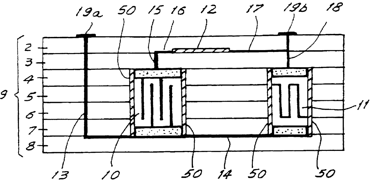
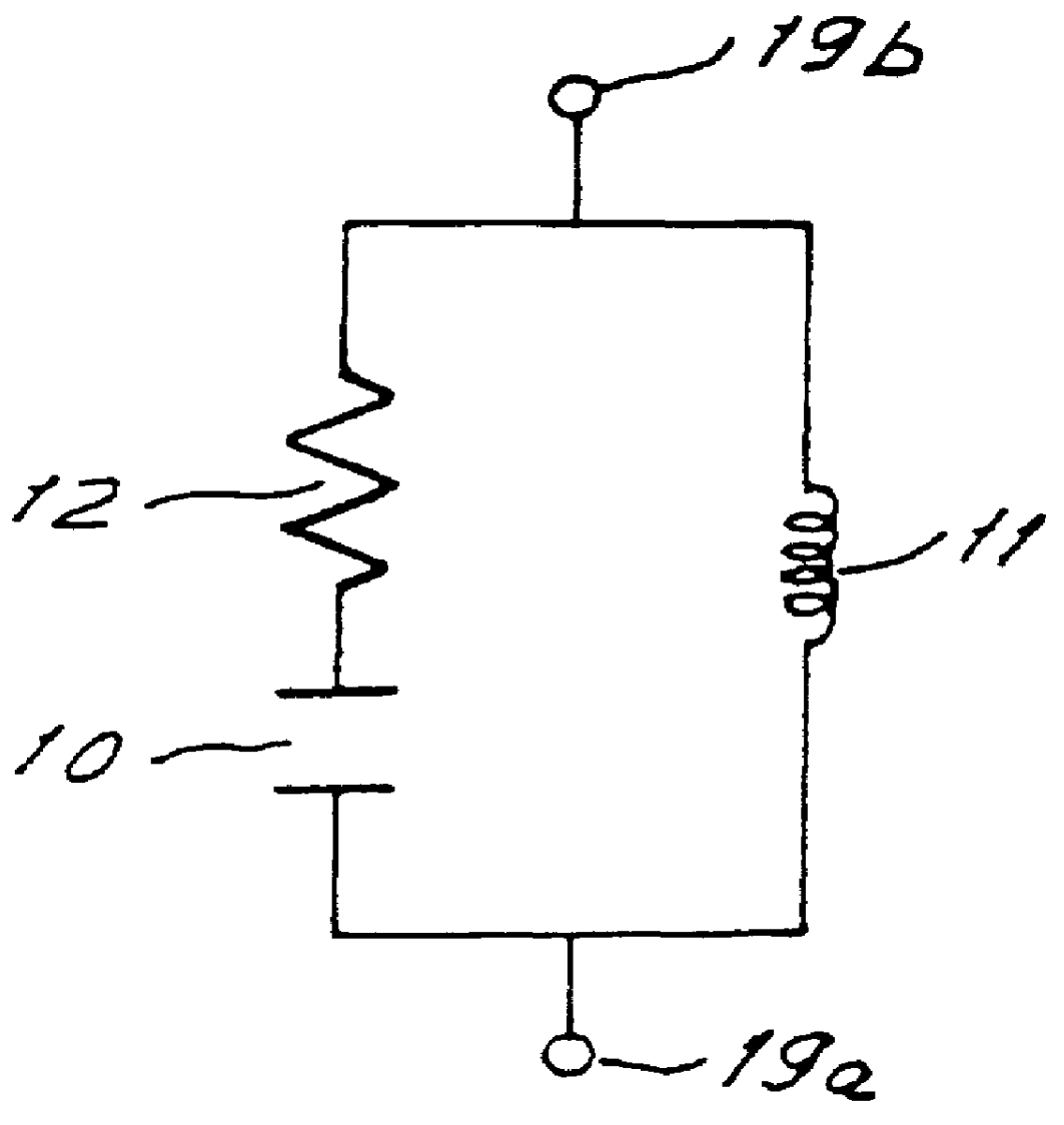
As shown in FIG. 1, the multi-layer ceramic substrate 1 includes a laminate 9 having a plurality of laminated ceramic layers 2, 3, 4, 5, 6, 7 and 8 formed of a ceramic insulating material. A capacitor 10, an inductor 11 and a resistor 12 are built into the laminate 9 as passive components. The laminate 9 is provided with wiring conductors 13, 14, 15, 16, 17 and 18 for completing wiring among the capacitor 10, the inductor 11 and the resistor 12, and outer terminal conductors 19a and 19b disposed on the outer surface of the multi-layer ceramic substrate 1. Thus, the multi-layer ceramic substrate 1 constitutes a circuit shown in FIG. 2.

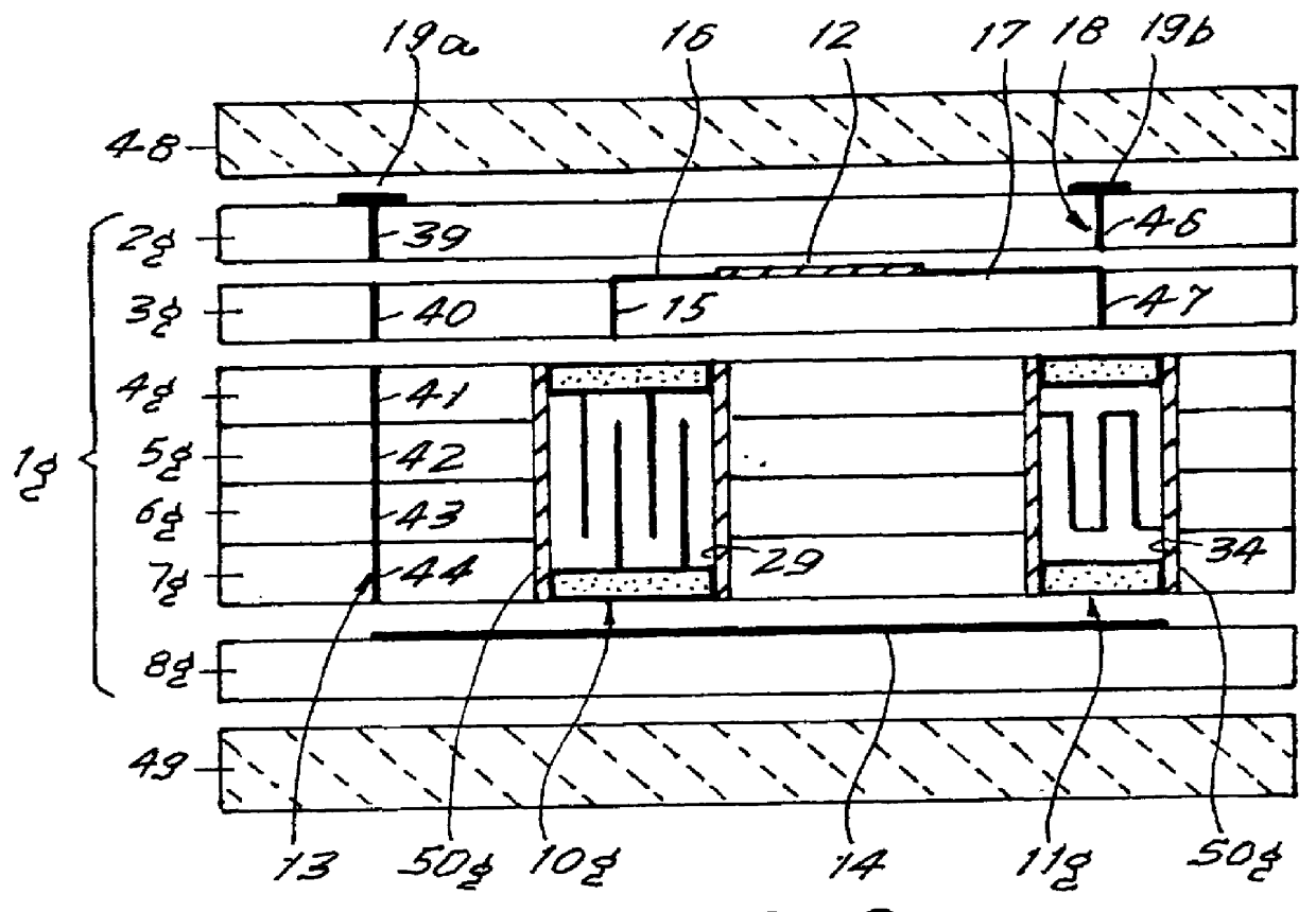
The multi-layer ceramic substrate 1 having the foregoing construction is produced as follows. FIG. 4 is a cross-sectional view for describing a method for obtaining some of the components shown in FIG. 3.

There are individually provided a compact block for producing a capacitor 10g containing a green ceramic functional material used for forming the above...


PUM

PropertyMeasurementUnit
firable temperatureaaaaaaaaaa
temperatureaaaaaaaaaa

Abstract

The present invention provides a method for producing a high-density multi-layer ceramic substrate with stable characteristics, the substrate incorporating therein a passive component such as a high-precision capacitor or inductor. The method comprises the steps of providing compact blocks containing a green ceramic functional material to form the passive components; providing a composite green laminate having a plurality of ceramic green sheets comprising a ceramic insulating material and in which the compact blocks are built in pre-disposed spaces and a paste containing a metal inducing, during firing, oxidation reaction accompanied by expansion is provided in space between inside walls of the spaces and the compact blocks; firing the composite green laminate in a state in which the laminate is sandwiched by the sheet-like supports formed of green ceramics that cannot be sintered at the sintering temperature, so as to prevent shrinkage of the laminate; and removing the unsintered sheet-like supports.

Description

1. Field of the InventionThe present invention relates to a multi-layer ceramic substrate and a method for producing the same, and more particularly, to a multi-layer ceramic substrate including passive components such as capacitors and inductors, and to a method for producing the same.2. Description of the Related ArtAs electronic devices have become smaller, there have generally been used ceramic substrates made of ceramic insulator and packed with various electronic components that constitute electronic circuitry. Recently, in order to attain an increased packing density and to meet high-frequency requirements, integral multi-layer ceramic substrates have been developed. These integral substrates are made by laminating a plurality of low dielectric constant ceramic sheets, each being provided with circuit patterns by use of paste containing a low-resistance conductive material such as Ag, Ag--Pd alloy, Cu, or Au, and firing the resultant laminate.To attain even higher packing den...

Claims


Application Information

Patent Timeline
Patent Type & Authority Patents(United States)
IPC IPC(8): H01L21/48H01L23/64H01L21/02H01L21/98H01L23/538H01L21/70H01L23/58H01L23/52H05K1/18H05K1/16H05K3/46
CPCH01L21/4857H01L23/642H01L23/645H01L25/50H05K1/16H05K1/185H01L23/5383Y10T428/24926H01L2924/09701H05K3/4629H05K2201/10636H01L2924/0002Y10T29/4913H01L2924/00Y02P70/50H05K3/46
Inventor SUNAHARA, HIROFUMI
Owner MURATA MFG CO LTD
Why Eureka
Try Eureka