Compound semiconductor device and method of manufacturing the same

a semiconductor device and compound technology, applied in the field of compound semiconductor devices, can solve the problems of poor reproducibility, inability to short gate and control the recess width, and difficult control and shorten the distance between the gate and the n.sup.+ region

Inactive Publication Date: 2001-01-30
NEC CORP
View PDF4 Cites 30 Cited by
  • Summary
  • Abstract
  • Description
  • Claims
  • Application Information

AI Technical Summary

Problems solved by technology

When a two-level recess is formed using two alignment processes, misalignment disadvantageously occurs, and the distance between the gate and the n.sup.+ region is difficult to control and shorten.
Even if the controllability in the lateral direction is improved using a multilayered mask, as disclosed in Japanese Unexamined Patent Publication No. 4-137737, etching also progresses along the lateral direction in recess etching, and a short gate and control of the recess width cannot be attained.
As for the direction of depth in recess etching, the recess depths at the first and second levels are controlled in terms of time, resulting in poor reproducibility, low controllability, and low uniformity.

Method used


Image

  • Compound semiconductor device and method of manufacturing the same
  • Compound semiconductor device and method of manufacturing the same
  • Compound semiconductor device and method of manufacturing the same

Examples


Embodiment Construction

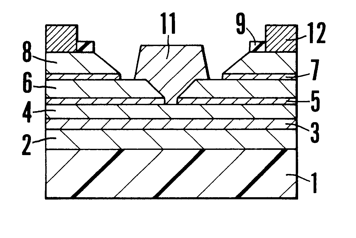
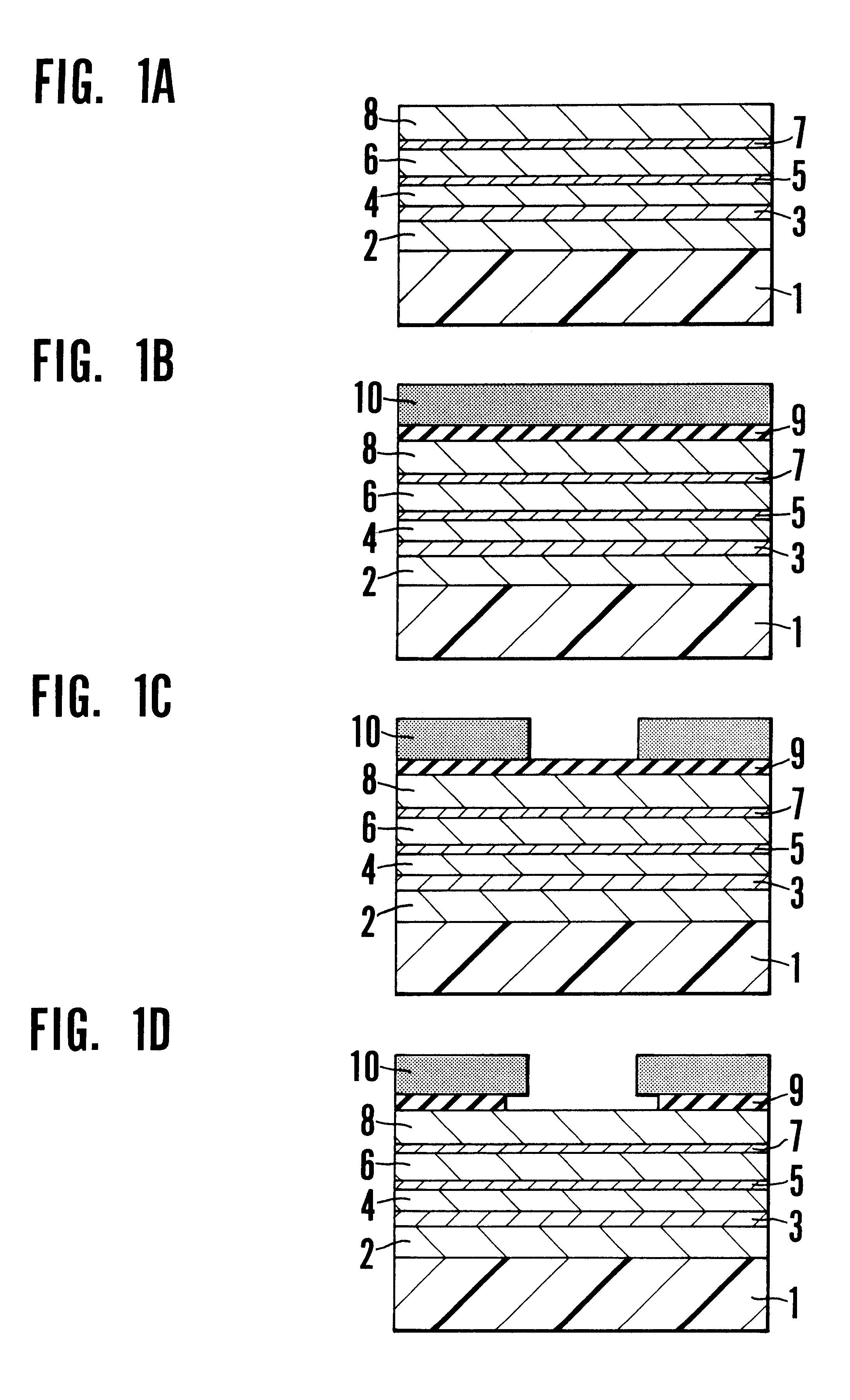
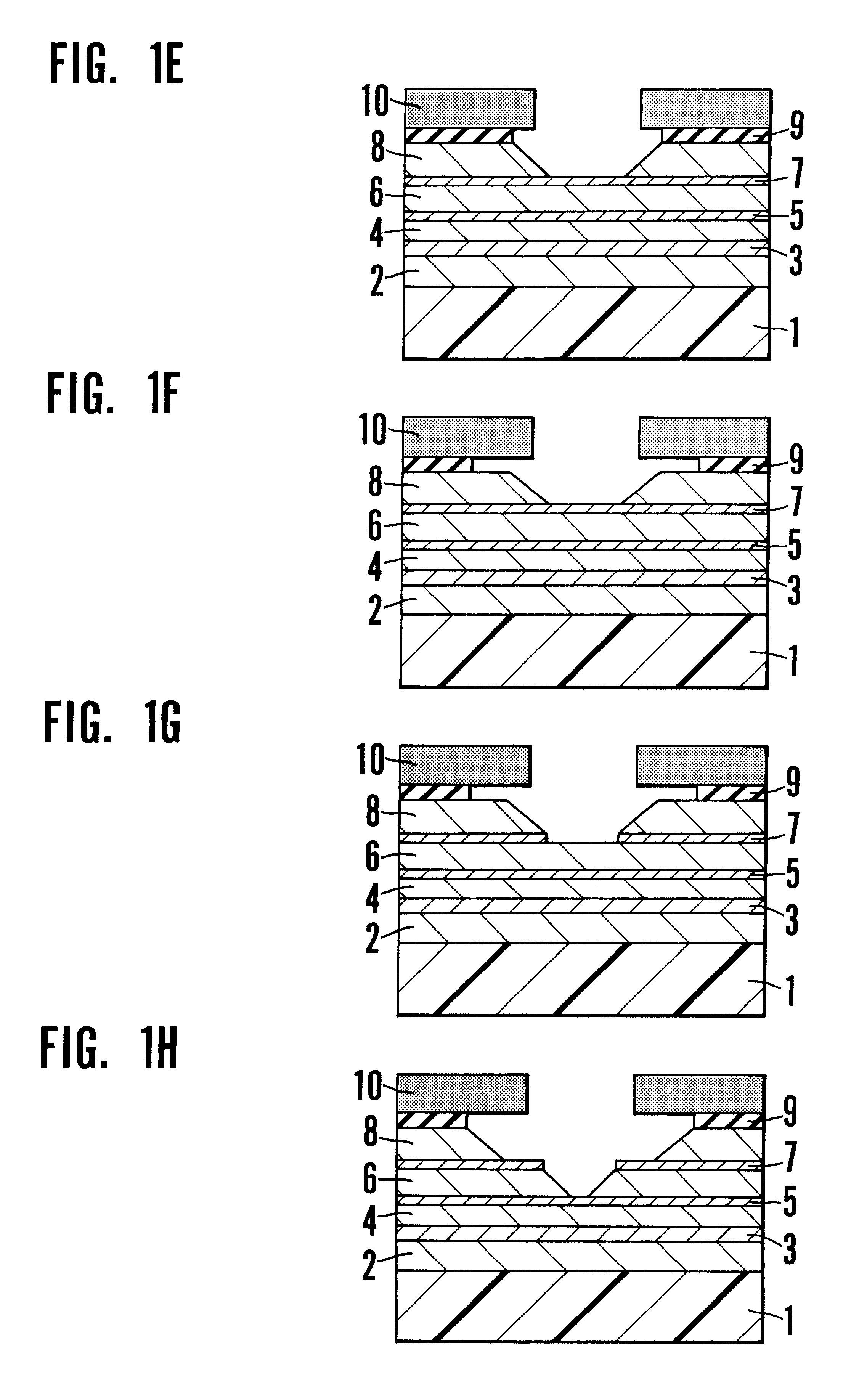
A heterojunction field effect transistor according to an embodiments of the present invention will be described below with reference to the accompanying drawings (FIGS. 1A to 1L).

As shown in FIG. 1A, a 500-nm i-GaAs buffer layer 2, a 15-nm i-InGaAs layer serving as a channel layer 3, and a 33-nm n-AlGaAs layer 4 having a carrier concentration of 2.times.10.sup.18 cm.sup.-3 are formed on a semi-insulating GaAs substrate 1 by, e.g., MOCVD from the substrate side. A 2-nm n-AlAs layer having a carrier concentration of 2.times.10.sup.18 cm.sup.-3 is formed as a first recess etching stopper layer 5 on the resultant structure. A 150-nm lightly doped n-GaAs layer having a carrier concentration of 1.times.10.sup.18 cm.sup.-3 is formed as a first semiconductor layer 6 on the first recess etching stopper layer 5. A 2-nm n-AlAs layer having a carrier concentration of 2.times.10.sup.18 cm.sup.-3 is formed as a second recess etching stopper layer 7 on the n-GaAs layer 6. A 50-nm heavily doped n-G...


PUM


Abstract

There are provided a compound semiconductor device having a semiconductor multilayered structure, and a method of manufacturing the same. The semiconductor multilayered structure consists of a first recess etching stopper formed on a conductive layer of a compound semiconductor, a first semiconductor layer formed on the first recess etching stopper layer, a second recess etching stopper layer formed on the first semiconductor layer, and a second semiconductor layer formed on the second recess etching stopper layer.

Description

1. Field of the InventionThe present invention relates to a compound semiconductor device and a method of manufacturing the same and, more particularly, to a field effect transistor having a multilevel recess structure and a method of manufacturing the same.2. Description of the Prior ArtWhen an LDD structure is to be realized with an HJFET in order to attain a higher gate breakdown voltage, a lower source resistance, and suppression of the short channel effect and the surface effect, a multilevel recess structure must be formed by performing recess etching in two stages upon two alignment processes in a conventional case. In Japanese Unexamined Patent Publication No. 4-137737, a multilayered mask is used to selectively side-etch the mask, thereby realizing a two-level recess structure with improved controllability in the lateral direction.When a two-level recess is formed using two alignment processes, misalignment disadvantageously occurs, and the distance between the gate and the...

Claims


Application Information

Patent Timeline
Patent Type & Authority Patents(United States)
IPC IPC(8): H01L29/778H01L21/285H01L21/02H01L21/335H01L29/66H01L21/28H01L21/306H01L21/338H01L29/41H01L29/812
CPCH01L21/28587H01L29/66462H01L29/7783H01L21/18
Inventor KASAHARA, KENSUKEOHNO, YASUOOHKUBO, SATORU
Owner NEC CORP
Why Eureka
Try Eureka