Flexible thin film ball grid array containing solder mask

a flexible, ball-grid array technology, applied in the field of thin-film ball-grid array flexible panels, can solve the problems of flexible flimsy film carrier panels that have a tendency to warp or bend, and tend to be warped or bent, and achieve the effect of removing the problem of distortion

Inactive Publication Date: 2001-02-13
IBM CORP
View PDF16 Cites 10 Cited by
  • Summary
  • Abstract
  • Description
  • Claims
  • Application Information

AI Technical Summary

Benefits of technology

The present invention makes it possible to use a mask reflow technique employing a solder mask, while at the same time significantly reducing, if not entirely eliminating the problem of distortion.
The present invention is also related to a method for fabricating the above disclosed electronic package. The method includes providing a flexible film carrier having electronic circuitry on both major surfaces thereof and a plurality of solder interconnection pads on a first major surface thereof. A solder mask layer is provided on both major surfaces of the flexible film carrier, whereby there exist areas between subsequently to be applied adjacent individual modules on the first major surface that are free from the solder mask. Modules having solder balls are located on the film corner with the solder balls being mated to corresponding solder interconnection pads. The solder balls are then subjected to reflow in order to bond the chips to the flexible film carrier. The absence of solder mask material in areas between adjacent individual modules significantly reduce the stress thereby reducing the distortion. The areas free from the solder mask material act as hinges relative to the stiff, slightly distorted portions that are not relieved. In addition, the presence of the solder mask on the second major surface of the flexible film carrier helps to strengthen the solder joint.

Problems solved by technology

Employing a C-4 type connection to attach a semi-conductor device to an organic flexible substrate presents fabrication problems.
In particular, because of the flexible nature of the organic substrates, they tend to warp or bend during processing and temperature fluctuations.
Although using a solder mask overcomes this problem, it has created another problem.
In particular, placing the solder mask on the flexible film carrier causes the flexible flimsy film carrier panel to badly distort.

Method used


Image

  • Flexible thin film ball grid array containing solder mask
  • Flexible thin film ball grid array containing solder mask
  • Flexible thin film ball grid array containing solder mask

Examples


Embodiment Construction

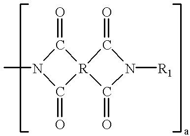
In order to facilitate an understanding of the present invention, reference still be made to the figures. The electronic package of the present invention includes a flexible film carrier 1 having electronic circuitry on both major surfaces (i.e., top and bottom) thereof (see FIG. 5 through 5). The flexible film carrier is a dielectric material and can be a thermal plastic or thermosetting organic resin.

Typical organic materials include conventional FR-4 epoxy and laminates based on high temperature resins such as high temperature epoxies, polyimides, cyanates (triazines), fluoropolymers, benzocyclobutenes, polyphenylene sulfides, polysulfones, polyetherimides, polyetherketones, polyphenylquinoxalines, polybenzoxazoles, and polyphenyl benzobisthiazoles.

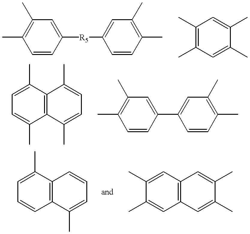
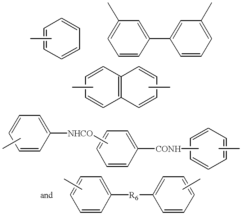
The preferred materials include the polyimides which can be unmodified polyimides, as well as modified polyimides, such as polyester imides, polyamide-imide-esters, polyamide-imides, polysiloxane-imides, as well as other mixed polyimid...


PUM


Abstract

An electronic package is provided that includes a flexible polyimide film carrier having electronic circuitry on both of its major surfaces and a plurality of solder interconnection pads on a first major surface; solder mask layers located on both major surfaces, provided that areas between subsequently to be applied individual circuit chips on the first major surface exist that are free from the solder mask; and a plurality of modules attached to the film carrier by the solder balls or bumps. Also provided is a method for fabricating the electronic package that includes reflow of the solder balls or bumps to achieve attachment of the modules.

Description

DESCRIPTION1. Technical FieldThe present invention is concerned with an electronic package and particularly concerned with a thin, ball grid array flexible panel, and method for its fabrication. More particularly, the present invention is concerned with a TBGA flexible panel that includes a solder mask and overcomes problem of distorting the flexible film carrier.2. Background ArtElectronic packages that include a thin film circuit member as an integral part thereof are known in the industry, with examples being defined in U.S. Pat. No. 4,849,856 to Funari et al., and U.S. Pat. No. 4,914,551 to Anschel et al., both of which are assigned to the same assignee as the present invention. In these electronic package structures, solder bonds are commonly used. In one technique, an electronic device or module (semiconductor chip) is mounted onto a packaging thin film structure in a "flip-chip" orientation. In this orientation, the surface of the chip having contact locations is placed facin...

Claims


Application Information

Patent Timeline
Patent Type & Authority Patents(United States)
IPC IPC(8): H01L23/498H01L23/48H05K3/34H05K1/11H05K3/00H05K1/00H01L21/60H01L23/12
CPCH01L23/49816H01L23/49838H01L23/4985H01L23/49894H05K1/112H05K3/3452H01L2924/12044H05K1/0393H05K3/0094H05K3/3457H05K3/3478H05K2201/0989H05K2201/10734H05K2203/041H05K2203/0455H05K2203/1394H05K2203/1572H01L2924/00013H01L2224/29099H01L2924/0002H01L2924/00H05K3/34
Inventor ARMEZZANI, GREGG JOSEPHIVES, ROBERT NICHOLASPIERSON, MARK VINCENTTULL, TERRY ALAN
Owner IBM CORP
Why Eureka
Try Eureka