Electrochemical etching method for silicon substrate having PN junction

a technology of etching method and silicon substrate, which is applied in the testing/measurement of individual semiconductor devices, semiconductor/solid-state devices, instruments, etc., can solve the problems of uneven characteristics of semiconductor pressure sensors and rough resultant etching surfa

Inactive Publication Date: 2001-02-27
DENSO CORP
View PDF28 Cites 6 Cited by
  • Summary
  • Abstract
  • Description
  • Claims
  • Application Information

AI Technical Summary

Benefits of technology

According to the present invention, though the etching surface has concave parts and convex parts when the formation of the anodic oxide film is equilibrated with the etching of the anodic oxide film on the etching surface on the PN junction part, the etching surface is smoothed by the subsequent voltage application. This is presumably for the reason that the anodic oxide film on the concave parts can not easily be etched and the anodic oxide film on the convex parts is easily etched on the concave parts and convex--parts of the etching surface, and as a result, the silicon on the convex parts is removed.

Problems solved by technology

However, due to the nature of the (110)-oriented silicon, this method results in the rough etching surface which causes unevenness to the characteristics of semiconductor pressure sensors.
However, this method of providing the SP--SiO.sub.2 film requires another component material in addition to the silicon substrate and additional processes.
Furthermore, even if electrochemical etching is used for etching the (110)-oriented silicon surface like etching a (100)-oriented silicon surface, the resultant etching surface is rough.

Method used


Image

  • Electrochemical etching method for silicon substrate having PN junction
  • Electrochemical etching method for silicon substrate having PN junction
  • Electrochemical etching method for silicon substrate having PN junction

Examples


first embodiment

This embodiment has embodied a semiconductor pressure sensor using a piezo-resistance layer.

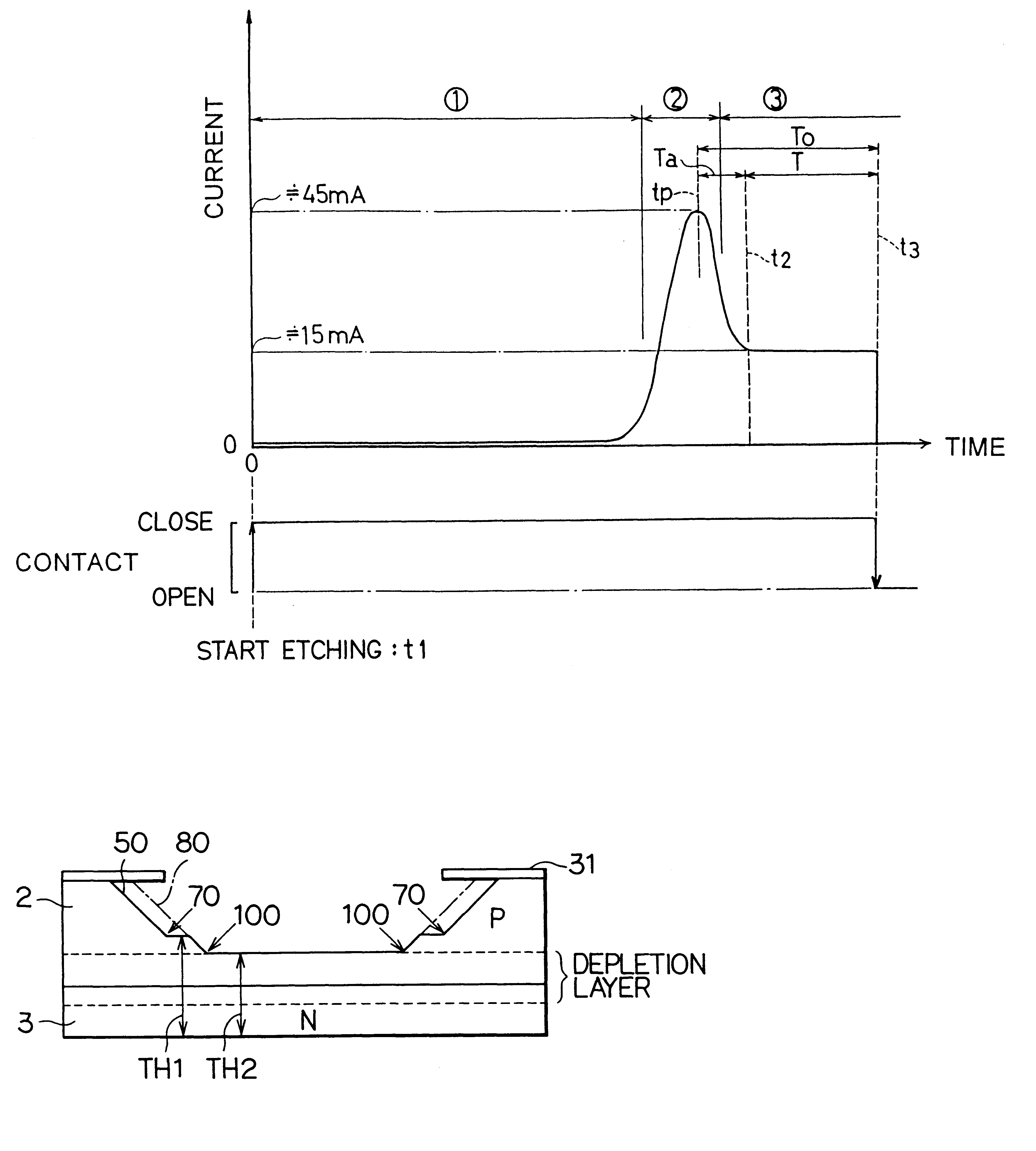
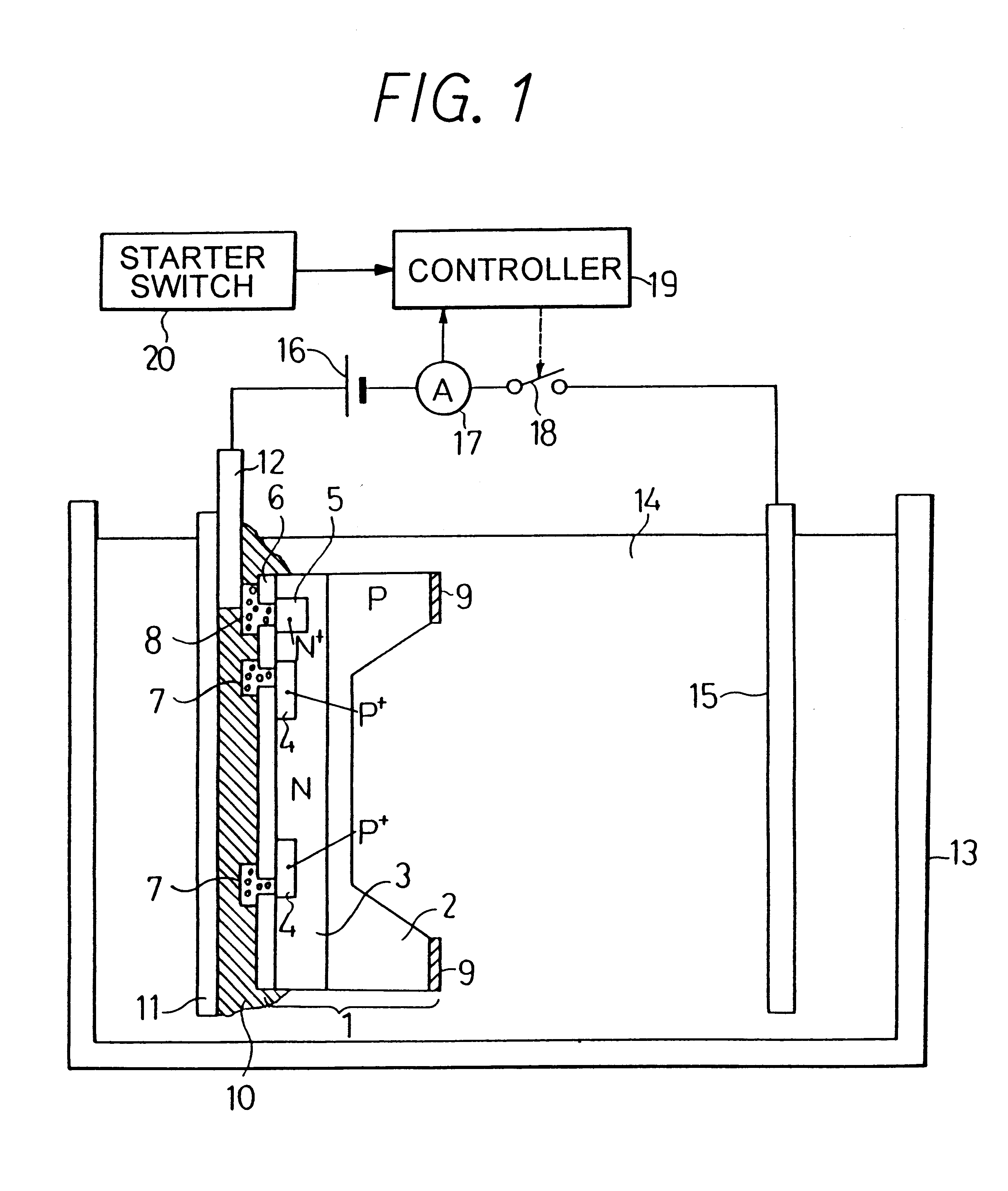
FIG. 1 is a schematic of an electrochemical etching system for forming a diaphragm on a silicon wafer 1. In the first place, description will be given to the silicon wafer 1. All over a (110)-oriented silicon substrate 2 of P-type is formed an N-type epitaxial layer 3. In the N-type epitaxial layer 3 is formed a P.sup.+ -type impurity diffusion layer 4 which serves as a piezo-resistance for sensing strain. In the N-type epitaxial layer 3 is also formed an N.sup.+ -type impurity diffusion layer 5 which enables the N-type epitaxial layer 3 to take an ohmic contact. Furthermore, on the N-type epitaxial layer 3 is formed a silicon oxide film 6. The P.sup.+ -type impurity diffusion layer 4 and the N.sup.+ -type impurity diffusion layer 5 are electrically drawn to the surface side of the silicon oxide film 6 by aluminum wiring 7 and 8.

On the surface of the silicon substrate where the N-type epitaxi...

second embodiment

Next, the second embodiment according to the present invention will be described focusing on the differences from the first embodiment.

In this embodiment, pulse voltage is applied as a voltage application method in overetching.

FIGS. 9 and 10 will be used for this description. FIG. 9 is the counterpart of FIG. 4, while FIG. 10 is the counterpart of FIG. 3.

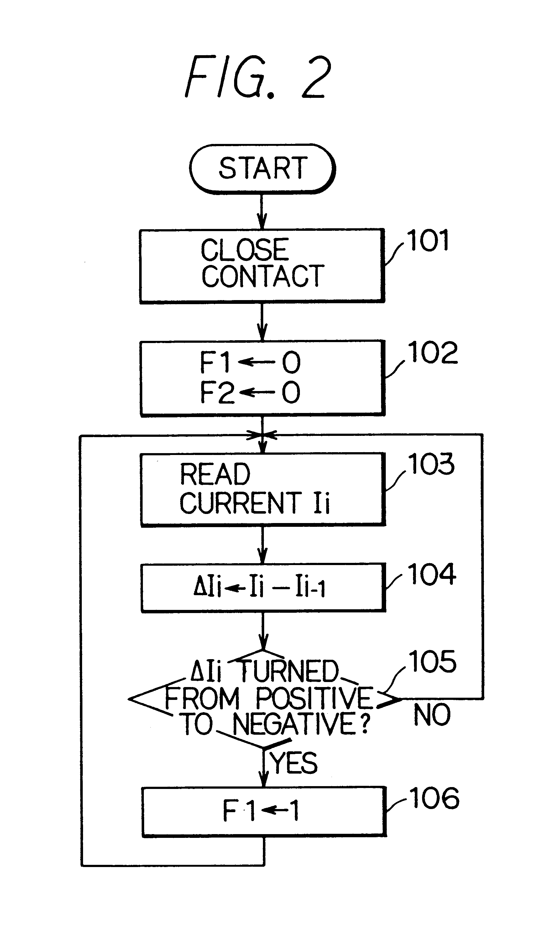
In FIG. 10, when the formation of the anodic oxide film formation is equilibrated with the etching of the anodic oxide film in Step 203, the controller 19 proceeds through Steps 204 and 205 to Step 207. In Step 207, the controller 19 sets the open / close operation mode of the contact 18. In this open / close operation mode, the controller 19 opens / closes the contact 18 as illustrated in FIG. 9. In this open / close operation, both the open time tx and close time ty of the contact 18 are 2.5 seconds respectively and the cycle tz is 5 seconds.

In this embodiment, as illustrated in FIG. 11A, the etching surface has triangular concave parts a...

third embodiment

Next, an application example of the first embodiment will be described.

This embodiment is an example in which the shapes of edge parts of the diaphragm are improvingly reformed to prevent the weakening thereof due to stress concentration thereon. Like the first embodiment described above, this embodiment is materialized in a form of a semiconductor pressure sensor using a piezo-resistance layer.

FIG. 14 is a cross-sectional view of the semiconductor pressure sensor according to this embodiment, and FIG. 15 is an enlarged view of a corner part of the diaphragm of the semiconductor pressure sensor of FIG. 14.

On a surface of the P-type (110)-oriented silicon substrate 2 is formed the N-type epitaxial layer 3 of 10 .mu.m thick, and of this stacked body is composed the silicon wafer 1. On the other surface of the P-type silicon substrate 2 is formed a first concave part 50 which is opened, and of a bottom surface 51 of the concave part 50 is composed of a thin part 60. A corner part 70 of...


PUM

PropertyMeasurementUnit
roughnessaaaaaaaaaa
roughnessaaaaaaaaaa
roughnessaaaaaaaaaa

Abstract

An etching method for a silicon substrate, which can easily smooth the etching surface of the (110)-oriented silicon, is disclosed. A container is filled with KOH solution. In the KOH solution is immersed a (110)-oriented silicon wafer having a PN junction and is also disposed a platinum electrode plate to face the silicon wafer. To between a platinum electrode of the silicon wafer and the platinum electrode plate are connected a constant voltage power source, an ammeter and a contact in series. A controller starts etching from one surface on which the PN junction is formed, and terminates voltage application when the specified time lapses after the formation of an anodic oxide film is equilibrated with the etching of the anodic oxide film on the etching surface on the PN junction part. In this case, the controller detects flowing current through the ammeter, and the point of time when the equilibrium state is obtained is the point of inflection of the detected current to the constant current after the peak thereof.

Description

1. Field of the InventionThe present invention generally relates to an etching method for silicon substrates. More particularly, the present invention relates to an etching method for silicon substrates used for forming thinned portions of semiconductor sensors, e.g., a pressure sensor and an acceleration sensor.2. Related ArtsIn the conventional technique of manufacturing semiconductor pressure sensors, anisotropic etching using KOH is used for forming a thin diaphragm on a portion of a (110)-oriented silicon substrate, i.e., the (110)-oriented silicon substrate is etched by KOH through time control. However, due to the nature of the (110)-oriented silicon, this method results in the rough etching surface which causes unevenness to the characteristics of semiconductor pressure sensors. For this reason, there has been a need to smooth the etching surface.As a solution to this problem, a SiO.sub.2 (SP--SiO.sub.2) film formed by the spattering method is provided on the etching surface...

Claims


Application Information

Patent Timeline
Patent Type & Authority Patents(United States)
IPC IPC(8): G01L9/00H01L29/66H01L29/84
CPCG01L9/0042H01L29/84Y10S438/977
Inventor SAKAI, MINEKAZUFUKADA, TSUYOSHITANIZAWA, YUKIHIKOMIZUNO, KOKISUZUKI, YASUTOSHIABE, YOSHITSUGUTANAKA, HIROSHIITO, MOTOKIIKEDA, KAZUHISAOKADA, HIROSHI
Owner DENSO CORP
Why Eureka
Try Eureka