Ion implantation method

a technology of ion implantation and ionization, which is applied in the direction of vacuum evaporation coating, coating, sputtering coating, etc., can solve the problems of reducing the productivity of the implant machine, reducing the performance of the resulting device, and amorphising the surface layer of the substra

Inactive Publication Date: 2001-03-13
APPLIED MATERIALS INC +1
View PDF17 Cites 34 Cited by
  • Summary
  • Abstract
  • Description
  • Claims
  • Application Information

AI Technical Summary

Problems solved by technology

A problem with ion implantation techniques is that a proportion of the ions entering the substrate at the desired implant energy penetrate into the substrate to a depth greater than would be expected from the calculations of the probability of experiencing a collision with an atom of the substrate material.
This problem is especially significant if it is intended to form the junction at a relatively shallow depth using low implant energies, as the extent of channelling is greater at lower energies.
A problem of this procedure is, however, that ...

Method used


Image

  • Ion implantation method
  • Ion implantation method

Examples


Embodiment Construction

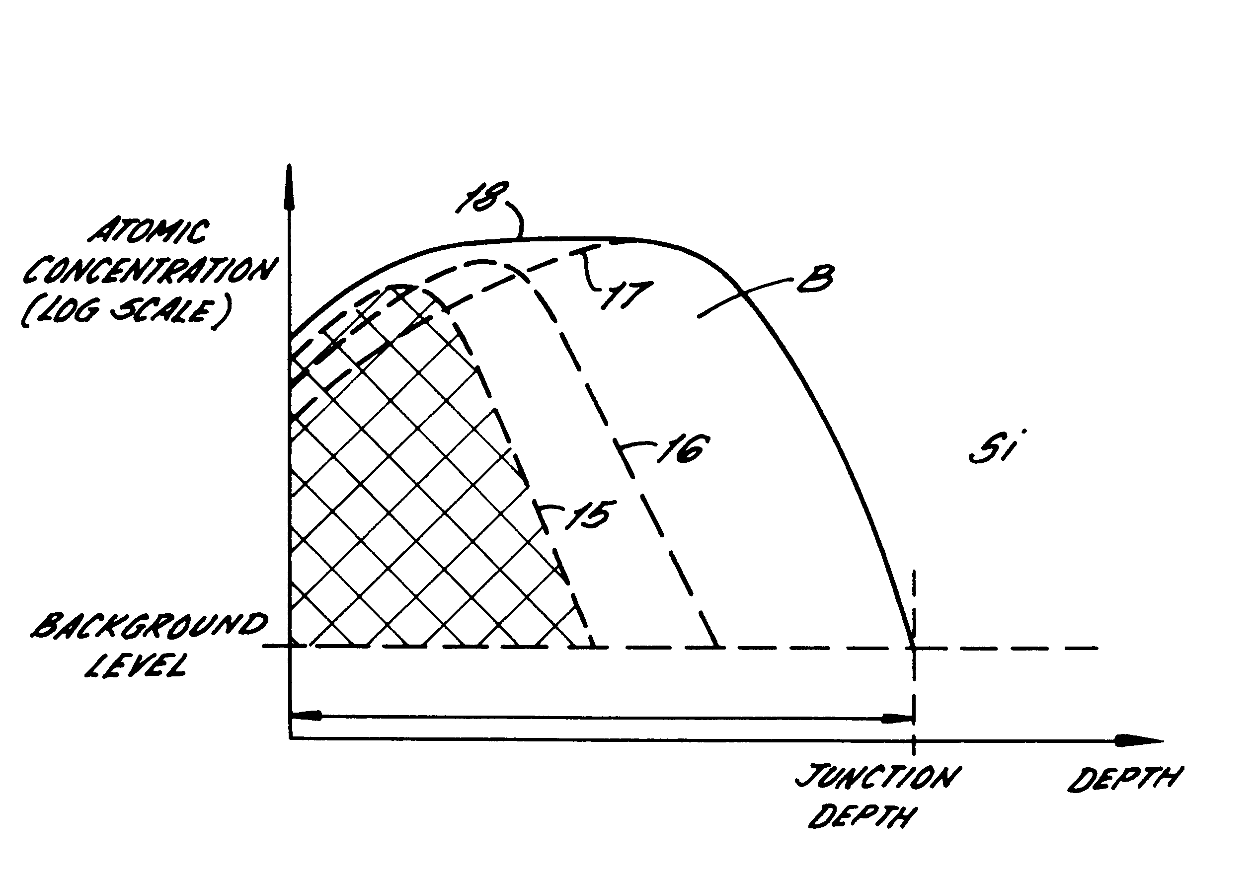
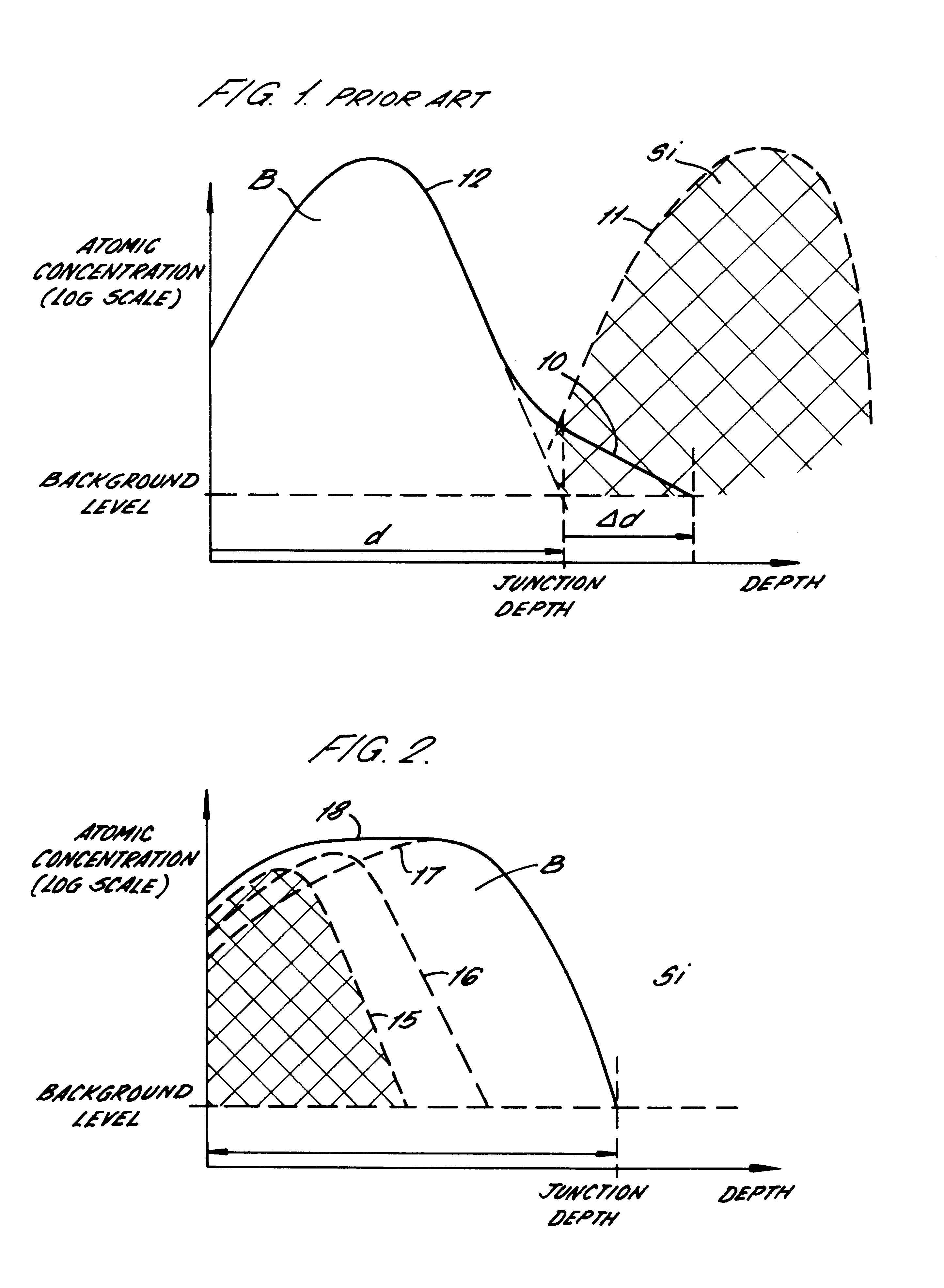
In FIG. 1, the effect of ion channelling during a known implantation processes is illustrated. If boron ions for example are implanted continuously at a predetermined energy, the concentration profile with depth of boron atoms in the silicon substrate has the shape of curve 12 in the drawing. Instead of the concentration dropping to the background level at the desired junction depth d within the substrate, a significant concentration of boron ions is formed at greater depths so that the effective junction depth is increased by .DELTA.d. The resulting profile of boron concentration has a so called channelling tail 10.

In the prior art, this effect has been ameliorated by performing a pre-implant at relatively high energy of silicon ions. The purpose of the silicon pre-implant is to amorphise the crystal structure of the silicon below the surface of the substrate. However the implanted silicon also dislocates and damages the crystal structure over a region illustrated in FIG. 1 by the ...


PUM

PropertyMeasurementUnit
Fractionaaaaaaaaaa
Fractionaaaaaaaaaa
Fractionaaaaaaaaaa

Abstract

In ion implantation processes for forming junctions in semiconductor devices, a proportion of ions implant into the semiconductor material beyond the desired junction depth due to channelling along axes and planes of symmetry in the crystal. A method is provided in which ions are implanted at a series of different energies starting with a lower energy than that required for the desired junction depth. The initial amorphising of the surface regions of the semiconductor during the lower energy implantation reduces the channelling probability when the ions are subsequently implanted at the full energy resulting in a more sharply defined junction.

Description

This invention relates to a method of ion implantation.DISCUSSION OF PRIOR ARTIon implantation is one of the standard processes employed in the manufacture of integrated circuit devices to modify the electrical properties of defined regions of a substrate of semiconductor material by doping these regions with a selected concentration of impurity atoms. The technique involves generating a beam of ions containing a preselected atomic specie and directing the beam towards a target substrate. The depth of implant of the atomic specie depends inter alia on the energy of the specie at implantation which is in turn dependent on the ion beam energy.There is an increasing demand for ion implantation to be conducted at lower implant energies so that junctions between regions of different conductivity type can be formed in the semiconductor substrate at shallow depths below the substrate surface. Such shallow junctions require implantation at implant energies of less than 10 keV and sometimes ...

Claims


Application Information

Patent Timeline
IPC IPC(8): C23C14/48H01L21/02H01L21/265
CPCC23C14/48H01L21/26513H01L21/26566H01L21/2658
Inventor TAYLOR, MITCHELL C.ADIBI, BABAKFOAD, MAJEED ALI
Owner APPLIED MATERIALS INC
Why Eureka
Try Eureka