Semiconductor integrated circuit device with low power consumption and simple manufacturing steps

a technology of integrated circuits and semiconductors, applied in logic circuits, logic circuits, logic functions, etc., can solve the problems of low operation speed of logical circuits, increased power consumption in sleep mode, and increased leakage current, so as to reduce the number of manufacturing steps and production costs

Inactive Publication Date: 2001-03-27
NEC CORP
View PDF13 Cites 116 Cited by
  • Summary
  • Abstract
  • Description
  • Claims
  • Application Information

AI Technical Summary

Benefits of technology

It is therefore an object of this invention to provide a semiconductor integrate

Problems solved by technology

Such a low source voltage results in a low operation speed of the logical circuit.
However, such a MISFET having a low-threshold voltage (Vt) suffers an increase in leakage current (hereinafter called off current) while the FET is nonconductive.
Therefore, in total power consumption of the logical circuit in an active mode and a sleep mode, the power consumption in the sleep mode tends to increase.
This results in increase in number of manufacturing steps.
This results in an unfavorable increase in layout area.
In addition, the operation of the data holding circuit is complicated as de

Method used


Image

  • Semiconductor integrated circuit device with low power consumption and simple manufacturing steps
  • Semiconductor integrated circuit device with low power consumption and simple manufacturing steps
  • Semiconductor integrated circuit device with low power consumption and simple manufacturing steps

Examples


first embodiment

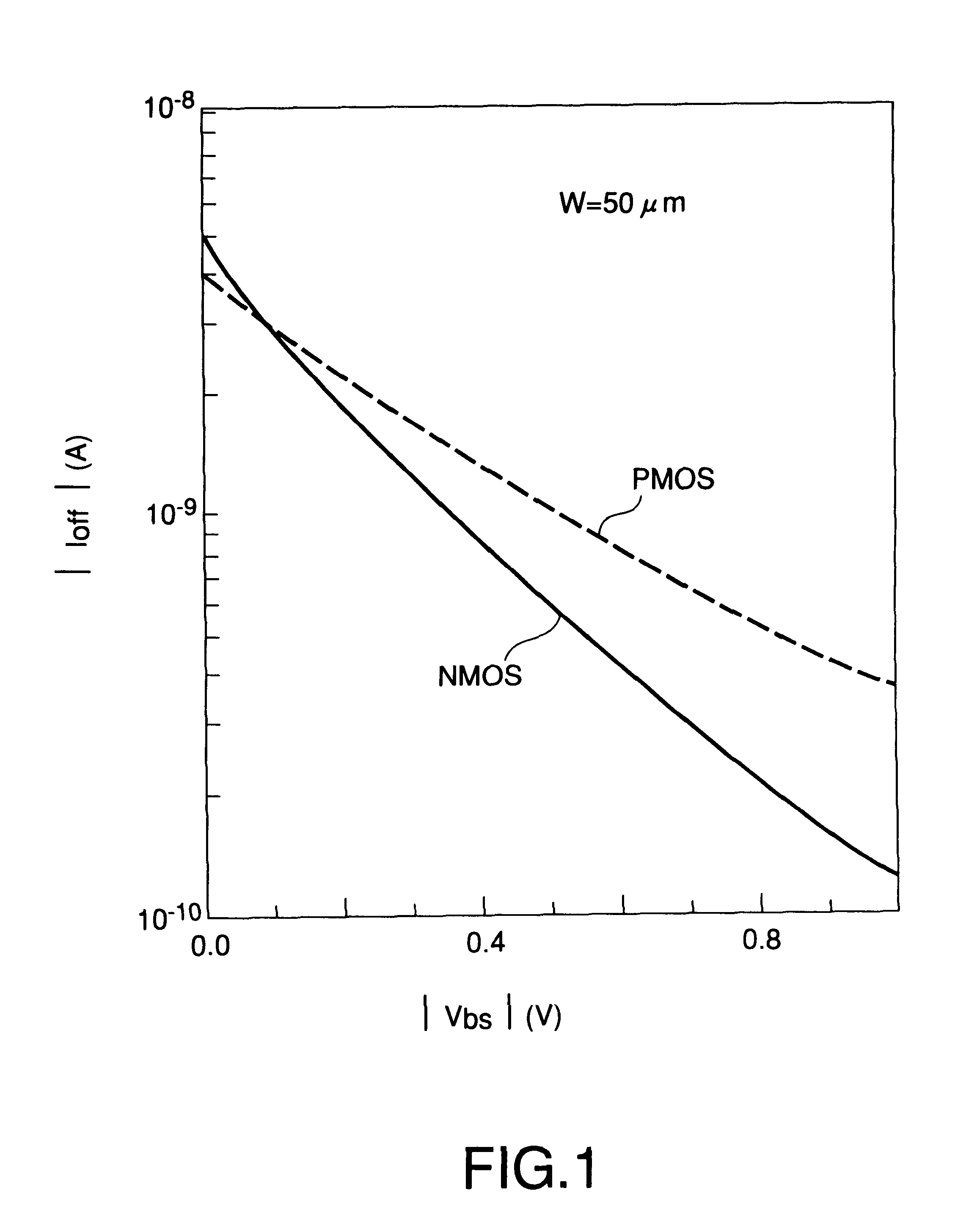
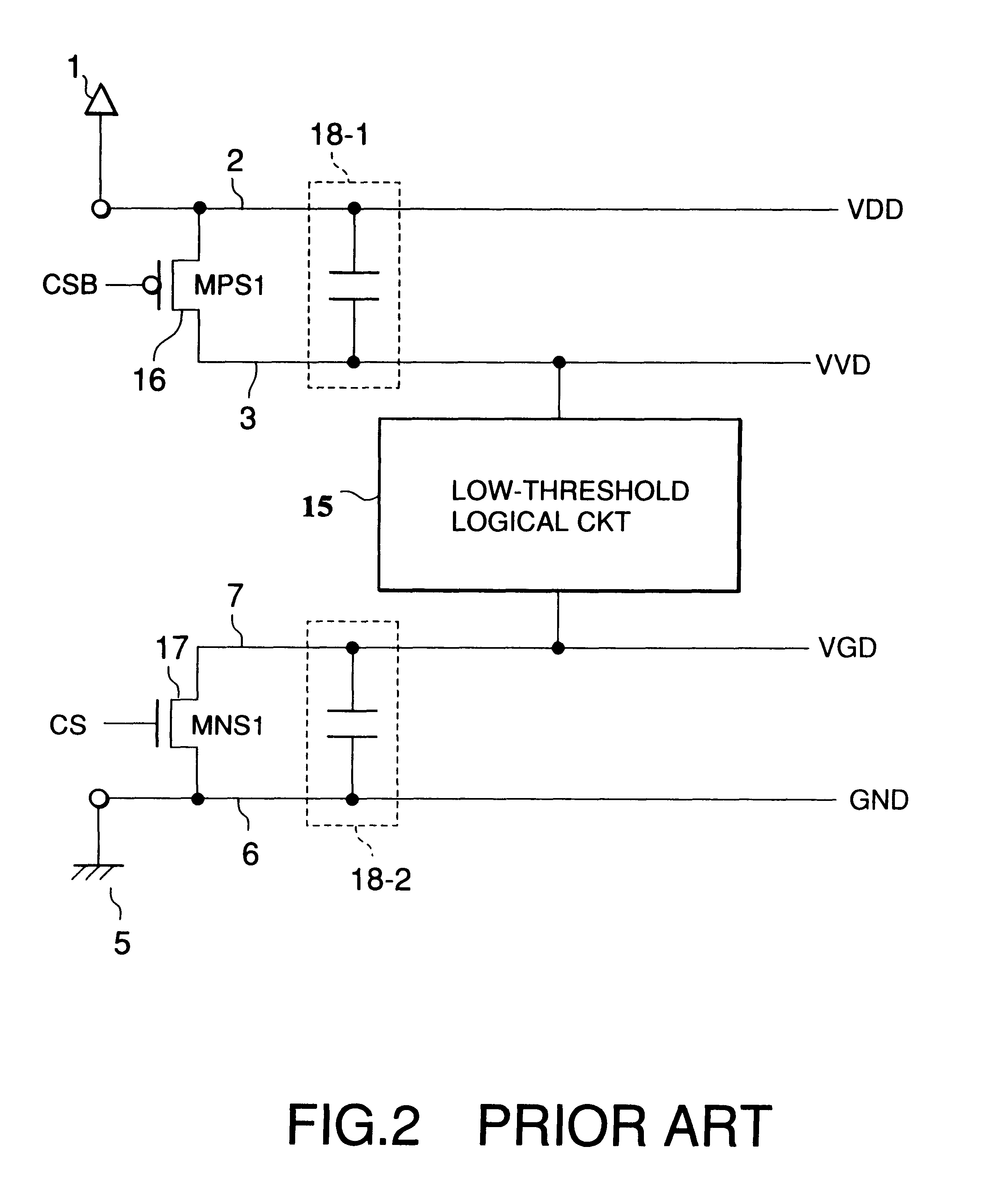
Referring to FIG. 5, a semiconductor integrated circuit according to this invention comprises a logical circuit 10, a first power supply switching circuit, and a second power supply switching circuit. The first power supply switching circuit comprises a first control transistor 4 and a first potential clamp circuit 9-1 and is arranged between a power supply line (VDD) 2 connected to a power supply 1 and a virtual power supply line (VVD) 3. Likewise, the second power supply switching circuit comprises a second control transistor 8 and a second potential clamp circuit 9-2 and is arranged between a grounding line (GND) 6 connected to the ground 5 and a virtual grounding line (VGD) 7. The logical circuit 10 has a first power supply terminal connected to the virtual power supply line (VVD) 3 and a second power supply terminal connected to the virtual grounding line (VGD) 7. The logical circuit 10 comprises P-channel and N-channel MOSFETs. All of substrate terminals of the P-channel MOSFE...

fourth embodiment

In the fourth embodiment, a potential difference is produced between the power supply line (VDD) 2 and the virtual power supply line (VVD) 3 by an electric current flowing through the first resistor 14-1 in the sleep mode. Likewise, a potential difference is produced between the grounding line (GND) 6 and the virtual grounding line (VGD) 7 by an electric current flowing through the second resistor 14-2 in the sleep mode. It is thus possible to apply the back bias to the MOSFETs forming the logical circuit 10.

In this embodiment, it is possible to form the potential clamp circuit of a simple structure by the use of the potential difference produced by the electric current flowing through each of the first and the second resistors 14-1 and 14-2 in the sleep mode.

Referring to FIG. 9, a semiconductor integrated circuit according to a fifth embodiment of this invention is similar to the second embodiment except that the first and the second potential clamp circuits comprise first and seco...

seventh embodiment

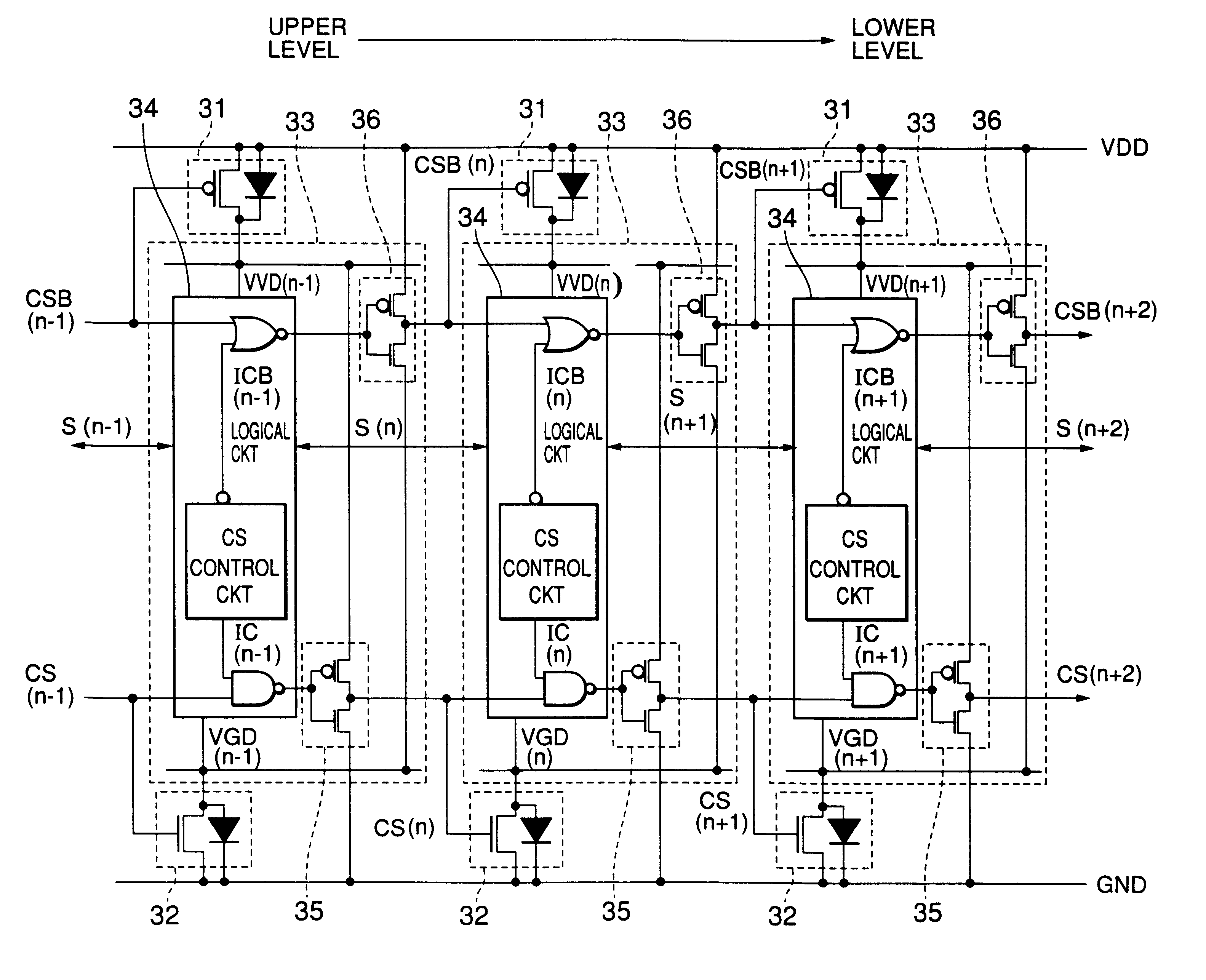
Referring to FIG. 11, a semiconductor integrated circuit according to this invention has a hierarchical structure comprising a plurality of circuits each of which is illustrated in FIG. 6.

As described in conjunction with FIG. 6, each of those circuits is provided with at least one of the first power supply switching circuit 31 comprising the first power supply switching transistor 4 connected between the power supply line (VDD) and the virtual power supply line (VVD) and the second power supply switching circuit 32 comprising the second power supply switching transistor 8 connected between the grounding line (GND) and the virtual grounding line (VGD). The active mode and the sleep mode are switched by turning on and off the power supply switching transistors. The seventh embodiment is directed to hierarchical control for the power supply switching transistors.

Referring to FIG. 11, an n-th level circuit group 33(n) is interposed between an (n-1)-th level circuit group 33(n-1) of an u...


PUM


Abstract

In a semiconductor integrated circuit, a control transistor 4 and a potential clamp circuit 9 are arranged between a power supply line 2 and a virtual power supply line 3. Even in a sleeve mode where the control transistor 4 is turned off, the potential clamp circuit 9-1 clamps the virtual power supply line 3 at a certain potential to hold a potential state (high level or low level) of each node of a logical circuit. At this time, each FET forming the logical circuit is applied with a back bias so that a threshold voltage Vt becomes higher than that in an active mode. Therefore, a leakage current can be decreased. In the semiconductor integrated circuit, the threshold voltage Vt of the control transistor 4 can be selected to be equal to that of one FET of the complementary FET forming the logical circuit. Therefore, the layout area and the number of manufacturing steps can be reduced.

Description

BACKGROUND OF THE INVENTIONThis invention relates to a semiconductor integrated circuit comprising low-threshold complementary MIS (Metal Insulator Semiconductor) field effect transistors and, in particular, to a circuit structure intended for reduced power consumption in a sleep mode.In a recent complementary MIS (Metal Insulator Semiconductor) logical LSI (Large-Scale Integrated circuit), each of MIS field effect transistors is reduced in gate length (L) so as to achieve an improvement in drivability of the transistor. Thus, an LSI chip having a high operation speed and a highly integrated structure is realized. With the reduction of the gate length (L), an operating source voltage is lowered in order to assure breakdown voltage and reliability of the transistor and to suppress the increase in power consumption of the whole chip due to the increase in device density.Such a low source voltage results in a low operation speed of the logical circuit. Taking this into account, each of...

Claims


Application Information

Patent Timeline
IPC IPC(8): H03K19/00
CPCH03K19/0016G11C11/40
Inventor KUMAGAI, KOUICHIKUROSAWA, SUSUMU
Owner NEC CORP
Why Eureka
Try Eureka