Electrostatic chuck and production method therefor

a technology of electrostatic chuck and production method, which is applied in the direction of electrostatic holding device, manufacturing tools, mechanical equipment, etc., can solve the problems of difficult to prepare ceramic plates having resistivity not less than 1 and the possibility of dielectric breakdown of minute circuits on the wafer

Inactive Publication Date: 2001-04-10
KYOCERA CORP
View PDF4 Cites 63 Cited by
  • Summary
  • Abstract
  • Description
  • Claims
  • Application Information

AI Technical Summary

Problems solved by technology

When the object to be held by the chuck is a semiconductor wafer, a minute circuit on the wafer may suffer from dielectric breakdown.
However, the resistivity of the ceramic portion is likely to vary, so that it is difficult to prepare a ceramic plate having a resistivity of not lower than 1.times.10.sup.9 .OMEGA.cm and lower than 1.times.10.sup.11 .OMEGA.cm in a temperature range of 250 to 450.degree. C.
This makes it impossible to ensure sufficient insulation in the case where an electrode for plasma generation is fixed to the under surface of the electrostatic chuck.
In the case of the electrostatic chuck which comprises a ceramic plate including a low resistivity ceramic portion and a high resistivity ceramic portion bonded to each other as disclosed in Japanese Unexamined Patent Publication No. 4-3956, sinter-bonding of the ceramic portions is difficult.
However, it is difficult to sinter-bond the ceramic portions for preparation of the ceramic plate because the ceramic portions, even if composed of the same principal ceramic material, have different thermal expansion coefficients and shrinkage degrees at firing thereof due to the presence of the impurity.

Method used


Image

  • Electrostatic chuck and production method therefor
  • Electrostatic chuck and production method therefor
  • Electrostatic chuck and production method therefor

Examples


Embodiment Construction

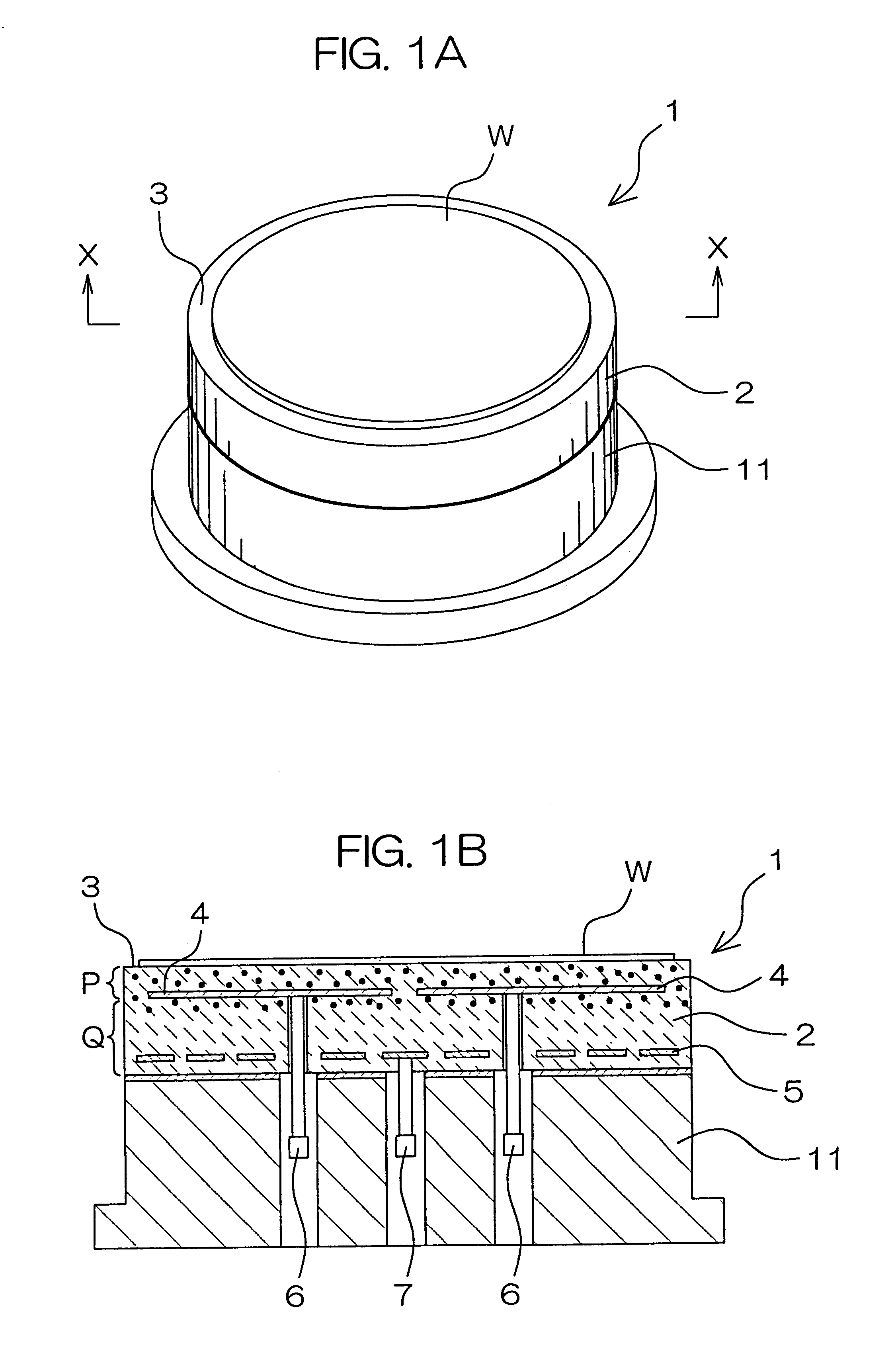
With reference to FIGS. 1A and 1B, an explanation will hereinafter be given to one specific example of the electrostatic chuck according to the present invention.

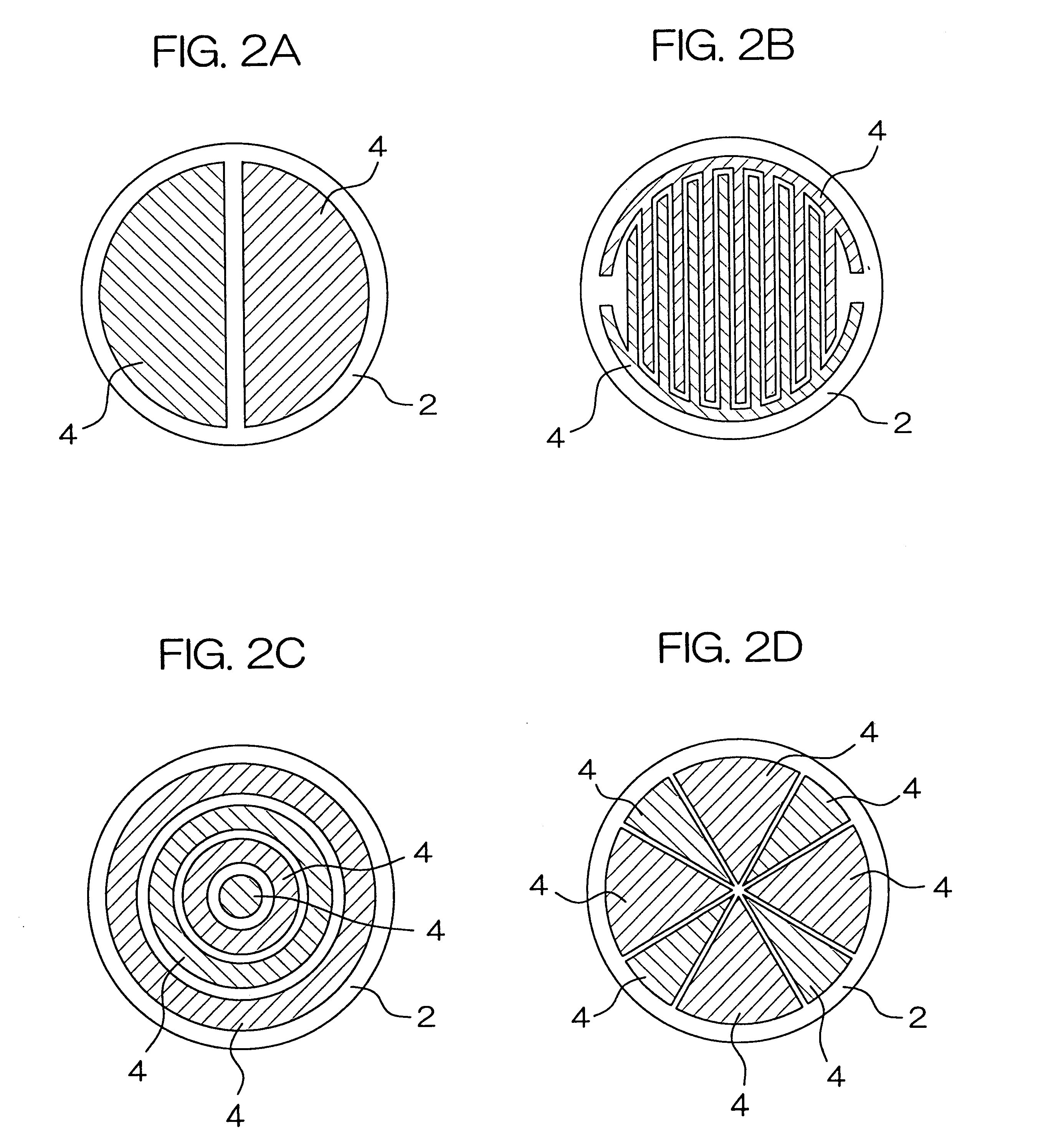
AlN powder having an average particle diameter of about 1.2 .mu.m and a purity of not lower than 99% was blended with a binder and a solvent for preparation of a paste. A plurality of green sheets each having a thickness of about 0.4 mm were formed from the paste by a doctor blade method. A conductive paste prepared by blending WC powder and AlN powder in a ratio of 7:3 and adjusting the viscosity of the resulting blend was applied in a pattern as shown in FIG. 2A on one of the green sheets for formation of electrostatic attraction electrodes 4, and in a pattern as shown in FIG. 3A on another of the green sheets for formation of a heating electrode 5, by means of screen printing, respectively.

After a binding liquid prepared by blending ethyl hexyl ether and diethyl phthalate in a ratio of 3:1 was applied on the respective g...


PUM

PropertyMeasurementUnit
thicknessaaaaaaaaaa
thicknessaaaaaaaaaa
temperatureaaaaaaaaaa

Abstract

An electrostatic chuck according to the present invention exhibits a greater attractive force by virtue of the Johnson-Rahbeck effect, while ensuring satisfactory insulation in a ceramic portion present below an electrostatic attraction electrode thereof in a temperature range of 250 to 450° C. The electrostatic chuck is produced by superposing green sheets printed with a conductive paste and green sheets not printed with the conductive paste in a predetermined order with a binding liquid applied on the respective green sheets, heat- and press-bonding the superposed green sheets and firing the heat- and press-bonded green sheets. During the production, a conductive component of the electrostatic attraction electrode is diffused into the ceramic portion present between the electrode and an attractive surface of the chuck.

Description

This application is based on an application No. 10-244282 filed in Japan, the content of which is incorporated hereinto by reference.1. Field of the InventionThe present invention relates to an electrostatic chuck for holding an object such as a semiconductor wafer by electrostatic attraction and to a production method therefor. More particularly, the invention relates to an electrostatic chuck exhibiting a great attractive force even in a high temperature environment and to a production method therefor.2. Description of the Prior ArtIn semiconductor-related production processes, electrostatic chucks are conventionally employed for holding a semiconductor wafer in a reaction process chamber with a high level of accuracy in semiconductor processing apparatuses such as film forming apparatuses for forming a thin film on a semiconductor wafer by PVD, CVD, sputtering and the like and dry etching apparatuses for microprocessing a wafer.In such a semiconductor processing apparatus, highly...

Claims


Application Information

Patent Timeline
Patent Type & Authority Patents(United States)
IPC IPC(8): H01L21/683H01L21/67H02N13/00
CPCH02N13/00H01L21/6833H01L21/6831Y10T279/23
Inventor NAGASAKI, KOICHI
Owner KYOCERA CORP
Why Eureka
Try Eureka