Periodically clearing thin film plasma processing system
- Summary
- Abstract
- Description
- Claims
- Application Information
AI Technical Summary
Benefits of technology
Problems solved by technology
Method used
Image
Examples
Embodiment Construction
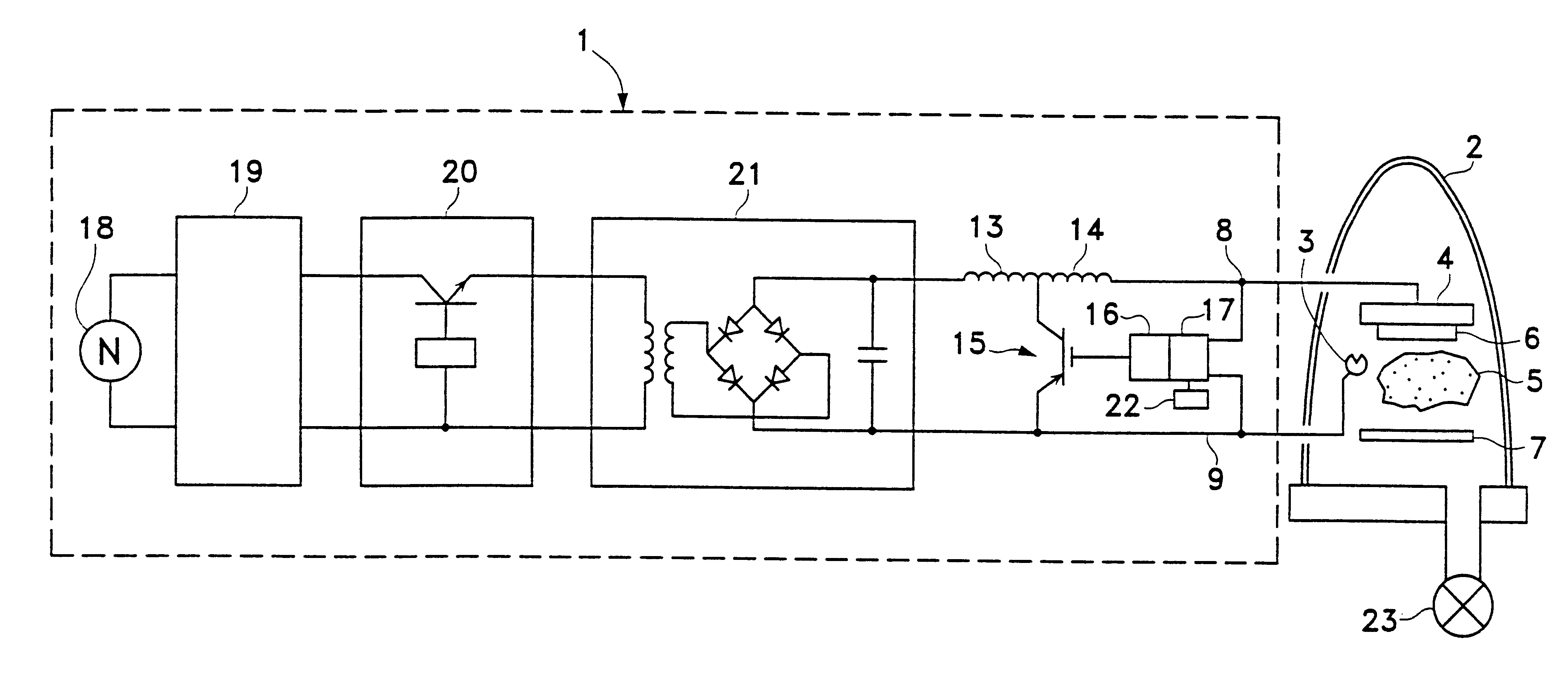
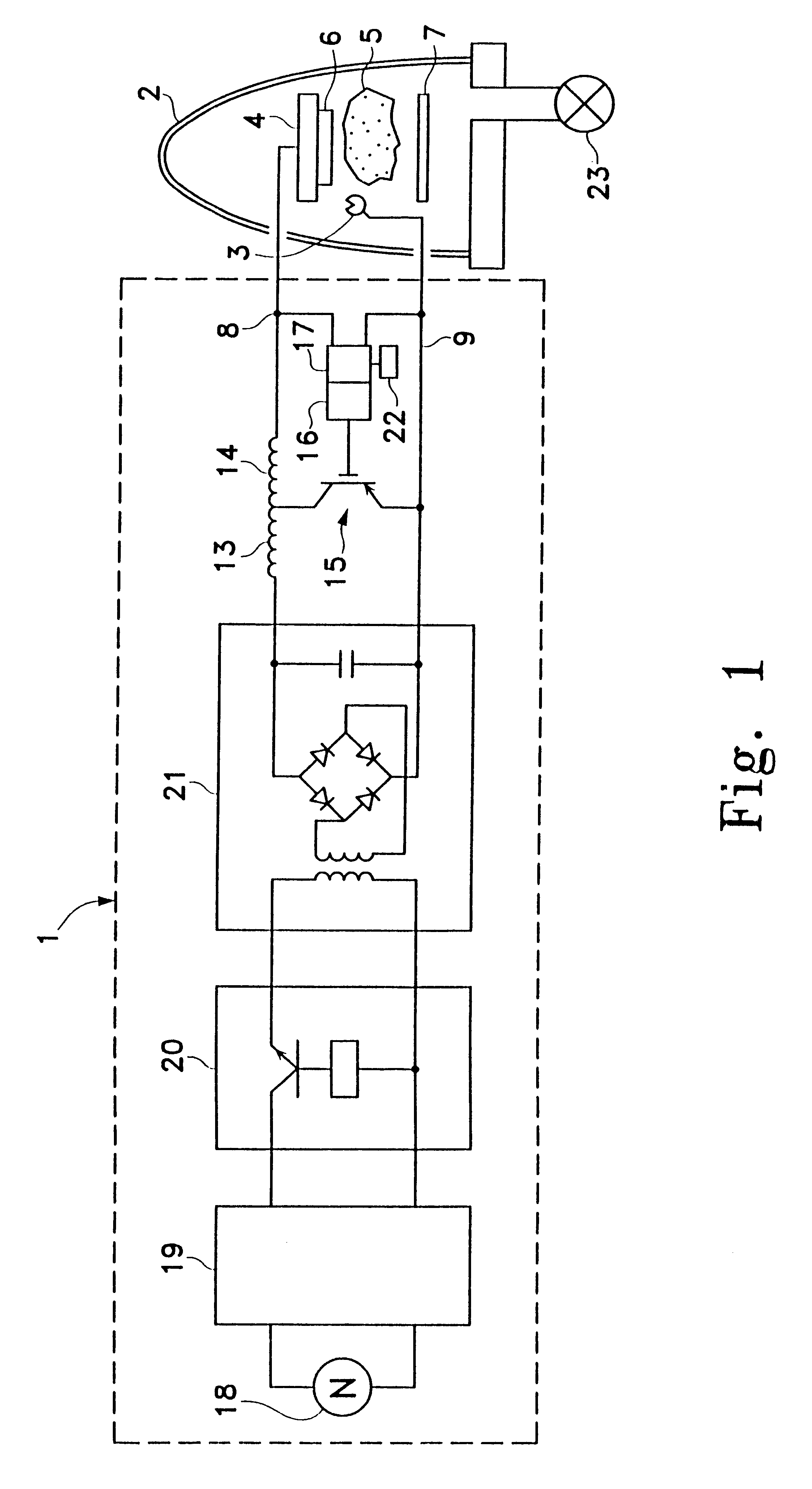
As will be readily understood, the basic concepts of the present invention may be embodied in a variety of ways. Referring to FIG. 1, the tapped inductor embodiment can be readily understood. In general, the DC plasma processing system includes the elements shown in FIG. 1. Specifically, DC power supply (1) is connected to coating chamber (2) within which cathode (4) and anode (3) are contained. In the deposition mode, the DC power supply (1) acts as a means for causing deposition of a coating material by creating an electric potential across cathode (4) and anode (3) to result in plasma (5). Plasma (5) then acts upon material target (6) so as to result in a coating on substrate (7). This coating may be the original target material or it may be the target material combined with some other elements such as reactive gas (23). Thus DC power supply (1) acts as a DC power source providing a direct current power output through first and second leads (8 & 9) into the plasma load to cause d...
PUM
| Property | Measurement | Unit |
|---|---|---|
| Time | aaaaa | aaaaa |
| Power | aaaaa | aaaaa |
| Current | aaaaa | aaaaa |
Abstract
Description
Claims
Application Information


