Photodiode with buffer layer

a photodiode and buffer layer technology, applied in the field of photodiodes, can solve the problems of increasing the installation cost of fibers, increasing the installation cost of optical couplers, and increasing the installation cost at subscribers

Inactive Publication Date: 2001-04-17
SUMITOMO ELECTRIC IND LTD
View PDF13 Cites 69 Cited by
  • Summary
  • Abstract
  • Description
  • Claims
  • Application Information

AI Technical Summary

Benefits of technology

When light with a long wavelength (h.nu.) enters a window layer (band gap is Eg.sub.1), if h.nu.<Eg.sub.1, the light transmits through the window layer and reaches an absorption layer. If the energy of the incident light (h.nu.) is higher than the band-gap energy of the absorption layer (Eg.sub.2)(Eg.sub.1 >h.nu.>Eg.sub.2), the light generates free electron-hole pairs there. Newly generated free electrons are attracted toward the n-side by a strong electric field, and holes toward the p-side, so that they are separated and cannot recombine. Respective flows of electrons toward the n-side region and holes toward the p-side region generate an electric current between the electrodes. This current is known as a photocurrent. This phenomenon makes it possible to convert light into an electric current to be detected.

Problems solved by technology

When two optical fibers are used, optical couplers are not necessary, but the cost for installing the fibers will increase.
However, optical couplers are expensive and increase the installation cost at subscribers.
The extremely thin absorption layer of a half-transmittance photodiode posed a new challenge.
It was difficult for the above-mentioned half-transmittance photodiode to operate stably in such a wide range of temperature.
With such a low voltage, p-n junctions sometimes do not receive sufficient voltage to operate normally.
This poor temperature characteristic deprives the invented half-transmittance photodiode of chances to be used outdoors or in cold climate.
With such a low voltage, the temperature characteristic is too poor for the photodiode to be used below 25.degree. C.
A light transmission and reception module with a half-transmittance photodiode and without an optical coupler will lose the usefulness thereof significantly if the module must be replaced by a combination of a conventional, complete-absorption-type photodiode and an optical coupler for outdoor or cold climate use.
However, diffusion cannot provide a sharp edge of distribution thereof.
Because zinc diffuses thermally, the density gradient cannot be sharp depthwise.
More specifically, zinc diffusion does not produce such a uniform high-density p.sup.+ -region as often explained in text books.
However, with the quaternary InGaAsP, the lattice matching cannot determine the composition exclusively.

Method used


Image

  • Photodiode with buffer layer
  • Photodiode with buffer layer
  • Photodiode with buffer layer

Examples


Embodiment Construction

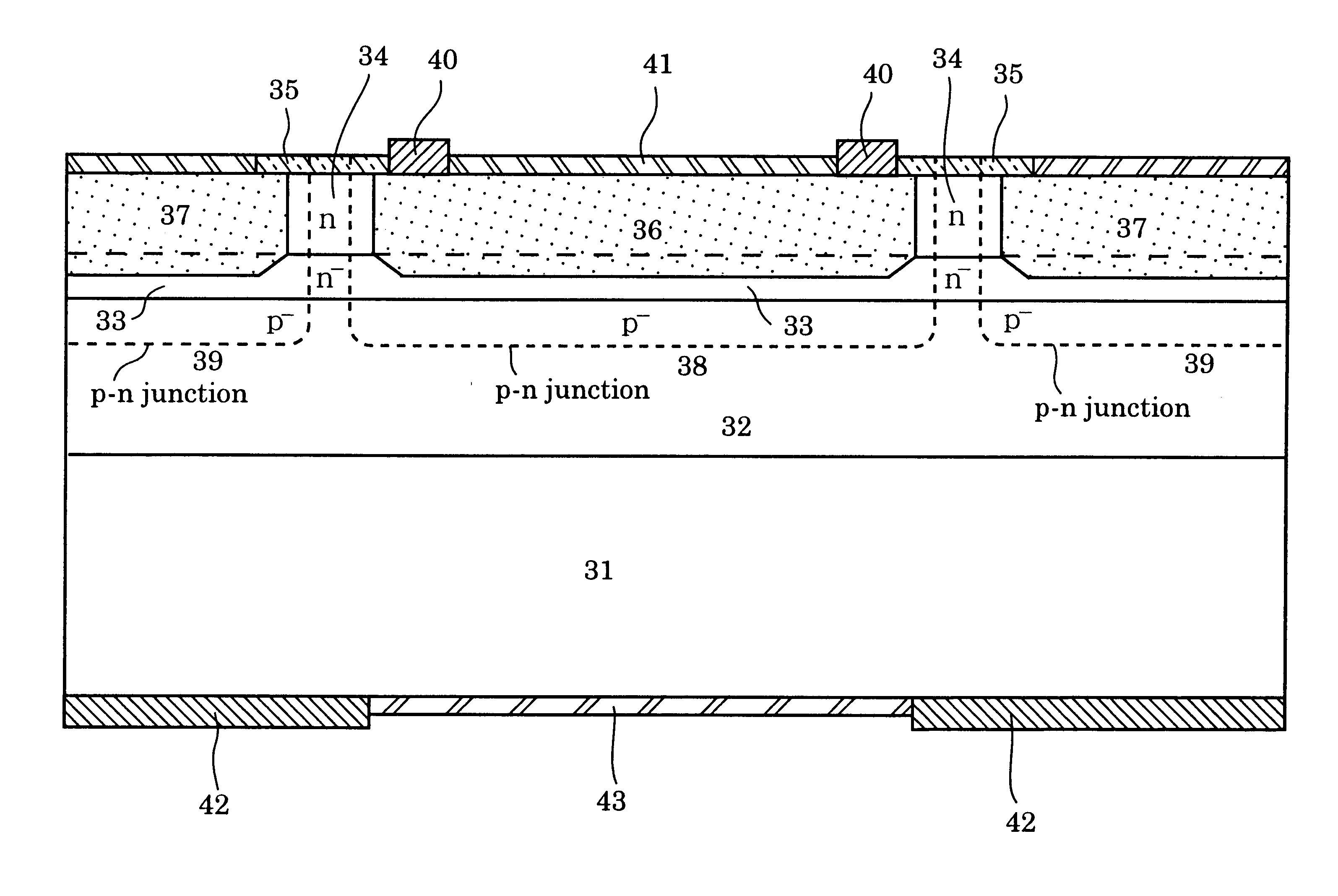
The following example has a quaternary-InGaAsP absorption layer with a fundamental absorption-edge wavelength of .lambda.g=1.42 .mu.m. As shown in FIG. 7, the absorption layer has thickness of 1 .mu.m to achieve 50-percent transmittance for a 1.31 .mu.m wave. When InGaAs is used as the absorption layer, the thickness should be 0.5 to 0.9 .mu.m to fulfill transmittance of 30 to 50%. Other aspects of the two materials are the same, and the following description is given on InGaAsP.

The concept of the present invention is well explained by comparing the layer thickness and impurity distribution shown in FIG. 7 with those in FIG. 3 for a conventional photodiode. A thinner absorption layer is one of the features of the invention. A thicker buffer layer, obtaining extra thickness from the decrement of the absorption-layer thickness, secures the formation of a p-n junction within the buffer layer.

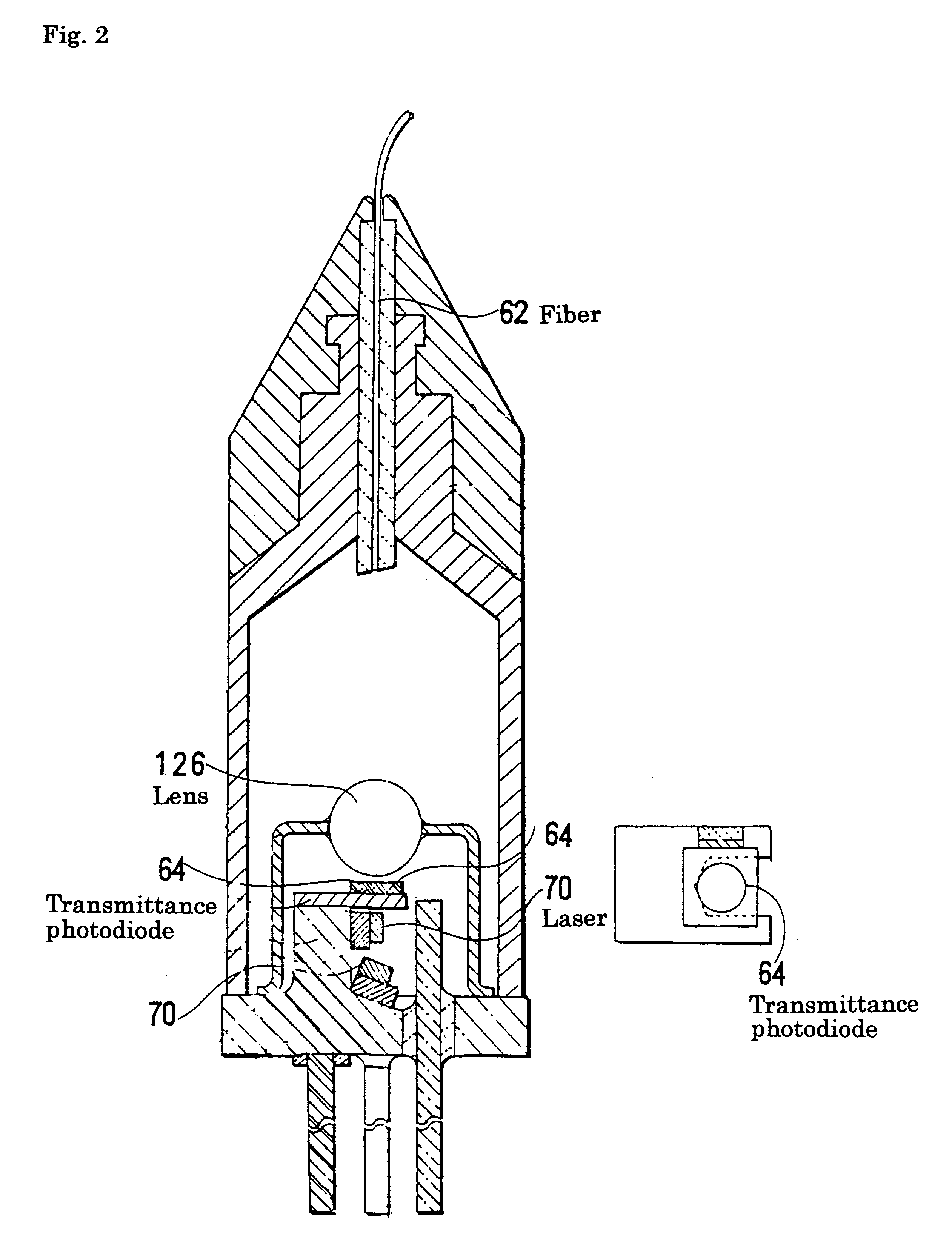
The structure shown in FIG. 7 is embodied in FIG. 8, which shows an actual structure of the hal...


PUM


Abstract

A half-transmittance photodiode usable as a photodetector in receivers for "ping-pong transmission" is improved in temperature characteristic, so that a half-transmittance photodiode usable at low temperatures is available. A p-n junction is formed in a buffer layer, not in an absorption layer.

Description

1. Field of the InventionThe present invention relates to a photodiode (PD) used in a system where light with a single wavelength is transmitted over a single optical fiber for bi-directional communications. More specifically, the invention relates to a photodiode used suitably for time-compression-multiplexing (TCM) transmission, or so-called "ping-pong transmission", based on time division using 1.3-.mu.m-region light for transmission and reception.2. Description of the Background ArtFIG. 1 is a diagram showing a simplified constitution of bi-directional communications. A laser diode LD1 at a central office sends an optical signal. An optical coupler 2 introduces the signal into a fiber 3, and an optical coupler 4 guides it to a photodiode PD2 at a subscriber, such as a house. This is downstream traffic. A signal from the subscriber is sent out by an LD2. The signal travels through the optical coupler 4, the fiber 3, and the optical coupler 2 and reaches a PD1 at the office. This ...

Claims


Application Information

Patent Timeline
Patent Type & Authority Patents(United States)
IPC IPC(8): H01L31/102H01L31/109H01L31/10
CPCH01L31/109
Inventor KUHARA, YOSHIKIIGUCHI, YASUHIROSAITO, TADASHITERAUCHI, HITOSHI
Owner SUMITOMO ELECTRIC IND LTD
Why Eureka
Try Eureka