Method for etching a trench having rounded top and bottom corners in a silicon substrate

a silicon substrate and trench technology, applied in the direction of basic electric elements, semiconductor/solid-state device manufacturing, electric devices, etc., can solve the problems of overlying deposited film layer electrical breakdown, high field stress in film, and edge leakag

Inactive Publication Date: 2001-05-22
APPLIED MATERIALS INC
View PDF5 Cites 301 Cited by
  • Summary
  • Abstract
  • Description
  • Claims
  • Application Information

AI Technical Summary

Problems solved by technology

These sharp, squared-off corners lead to high field stress in film layers subsequently deposited thereon during further processing steps.
The high field stress can potentially lead to the electrical breakdown of the overlying deposited film layers.
Further, the sharp, squared-off corners are a point of charge accumulation, which can cause edge leakage.
However, rounding of the corners in a manner which results in a loss of device active area is undesirable.
A sharp corner at the bottom of a trench can also be a source stress, causing problems of the kind described with reference to the top corners of the trench.
In general, a fast silicon oxide etch rate is not desired, because the silicon oxide layer is so thin that etching is completed quickly even if the silicon oxide etch rate is relatively low, and it is desired to provide time to permit formation of the polymer-oxide combination build-up adjacent the sidewall of the etched silicon oxide layer during the silicon oxide breakthrough etch step.
However, the first top corner rounding method is not intended to be limited to use of this specific apparatus.

Method used


Image

  • Method for etching a trench having rounded top and bottom corners in a silicon substrate
  • Method for etching a trench having rounded top and bottom corners in a silicon substrate
  • Method for etching a trench having rounded top and bottom corners in a silicon substrate

Examples


example two

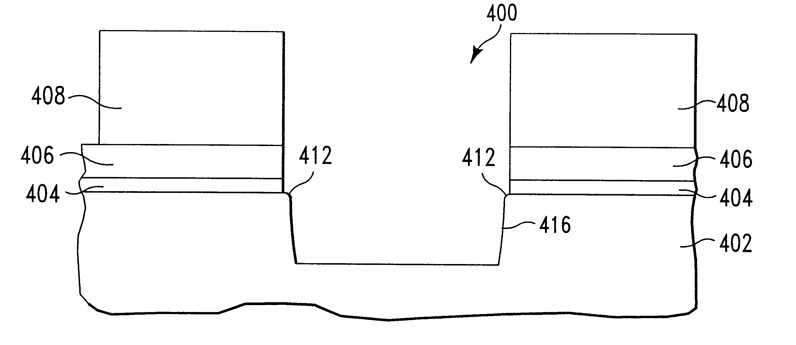
The semiconductor structure 500 shown in FIG. 5A was the starting substrate for the second top corner rounding method. This structure includes the silicon nitride hard mask 506, and silicon oxide layer 504, deposited on a single-crystal silicon substrate 502, as previously described. The silicon nitride masking layer 506 had a thickness of approximately 2,000 .ANG.. The silicon oxide layer 504 had a thickness of approximately 150 .ANG..

The silicon oxide break-through step which also formed extension 508 was performed using a plasma generated from a plasma feed gas containing 40 sccm CF.sub.4, 75 sccm argon, and either 50 sccm CH.sub.2 F.sub.2 or 70 sccm HBr. The silicon oxide breakthrough step was performed using the following process conditions: 70 mTorr process chamber pressure; 1200 W source power; 70 W (-335 V) bias power; and 20.degree. C. substrate temperature.

FIG. 5B shows the structure 500 of FIG. 5A following the silicon oxide breakthrough step. There was a critical dimensi...

example three

A two-step silicon etch process was then performed to provide a trench with a rounded bottom. In the first silicon etch step, the trench was etched to a depth of 2,500 .ANG. using 90 sccm Cl.sub.2 and 5 sccm O.sub.2. The first silicon etch step was performed using the following process conditions: 25 mTorr process chamber pressure; 1000 W source power; 200 W (-500 V) bias power; and 20.degree. C. substrate temperature.

In the second silicon etch step, the trench was etched to a final depth of 3,000 .ANG. using 90 sccm Cl.sub.2, 5 sccm O.sub.2, and 10 sccm SF.sub.6. The second silicon etch step was performed using the following process conditions: 55 mTorr process chamber pressure; 1000 W source power; 200 W (-520 V) bias power; and 20.degree. C. substrate temperature. The increased process chamber pressure, in combination with the presence of SF.sub.6, during the second silicon etch step enhanced the lateral etching, resulting in rounding of the bottom trench corners.

Using prior art ...


PUM

PropertyMeasurementUnit
pressureaaaaaaaaaa
pressureaaaaaaaaaa
sidewall angleaaaaaaaaaa

Abstract

The present invention provides straight forward methods for plasma etching a trench having rounded top corners, or rounded bottom corners, or both in a silicon substrate. A first method for creating a rounded top corner on the etched silicon trench comprises etching both an overlying silicon oxide layer and an upper portion of the silicon substrate during a "break-through" step which immediately precedes the step in which the silicon trench is etched. The plasma feed gas for the break-through step comprises carbon and fluorine. In this method, the photoresist layer used to pattern the etch stack is preferably not removed prior to the break-through etching step. Subsequent to the break-through step, a trench is etched to a desired depth in the silicon substrate using a different plasma feed gas composition. A second method for creating a rounded top corner on the etched silicon trench comprises formation of a built-up extension on the sidewall of an overlying patterned silicon nitride hard mask during etch (break-through) of a silicon oxide adhesion layer which lies between the hard mask and a silicone substrate. The built-up extension upon the silicon nitride sidewall acts as a sacrificial masking material during etch of the silicon trench, delaying etching of the silicon at the outer edges of the top of the trench. This permits completion of trench etching with delayed etching of the top corner of the trench and provides a more gentle rounding (increased radius) at the top corners of the trench. During the etching of the silicon trench to its final dimensions, it is desirable to round the bottom corners of the finished silicon trench. We have discovered that a more rounded bottom trench corner is obtained using a two-step silicon etch process where the second step of the process is carried out at a higher process chamber pressure than the first step.

Description

1. Field of the InventionThe present invention pertains to a method for etching a trench in a silicon substrate. In particular, the present invention pertains to particular plasma etch chemistries and process conditions which may be used to produce a rounded top trench corner, a rounded bottom trench corner, or both.2. Brief Description of the Background ArtTrenches formed in silicon using traditional etching methods typically have sharp, squared-off top corners. These sharp, squared-off corners lead to high field stress in film layers subsequently deposited thereon during further processing steps. The high field stress can potentially lead to the electrical breakdown of the overlying deposited film layers. Further, the sharp, squared-off corners are a point of charge accumulation, which can cause edge leakage. Rounding of the top corners in trench structures can be critical for device performance. However, rounding of the corners in a manner which results in a loss of device active...

Claims


Application Information

Patent Timeline
Patent Type & Authority Patents(United States)
IPC IPC(8): H01L21/70H01L21/02H01L21/308H01L21/762H01L21/3065
CPCH01L21/3065H01L21/3081H01L21/76232
Inventor MUI, DAVIDPODLESNIK, DRAGANLIU, WEILEE, GENEKIM, NAM-HUNCHINN, JEFF
Owner APPLIED MATERIALS INC
Why Eureka
Try Eureka