Thermal modulation system and method for locating a circuit defect such as a short or incipient open independent of a circuit geometry

a technology of circuit geometry and modulation system, which is applied in the direction of individual semiconductor device testing, instruments, and therapy, etc., can solve the problems of unstable structure of incipient defects, unwanted short circuit connections, and wide range of electrical resistan

Inactive Publication Date: 2001-05-22
GLOBALFOUNDRIES INC
View PDF20 Cites 4 Cited by
  • Summary
  • Abstract
  • Description
  • Claims
  • Application Information

AI Technical Summary

Benefits of technology

Still a further object invention is to provide a system and method capable of efficiently and accurately locating a circuit defect anywhere in a "search region" of an electric workpiece. In the default case, the search region includes the entire surface of the workpiece. In other cases, the original search region may be smaller, because the circuit is restricted to some part of the workpiece. According to the invention, circuit defects include, but are not limited to the following: a "short" defect, i.e., an unintended electrical connection, e.g. formed between plural circuit elements which otherwise would be unconnected; and, an "incipient open" defect which is typically an unintended resistive zone interposed in an otherwise conductive circuit. This resistive zone typically may be caused by abnormal geometry, or a crack, or abnormal material properties, or many other reasons. It is valuable to locate a defect, in order to analyze its structure and diagnose its cause, so that fabrication quality may be improved.
According to the preferred embodiments, the invention functions in accordance with the following principles: (1) Given a workpiece with an electric circuit which may have a circuit defect at an unknown location within a search region with many possible locations, the defect is efficiently and accurately located; (2) A circuit defect typically includes a resistive zone. When the zone changes temperature, its resistance changes slightly. When this is part of a circuit, the overall circuit resistance changes slightly. By contrast, for a perfect circuit, the resistance is much less sensitive to local temperature; (3) The relatively small resistance changes are more easily measured by using a time-modulated stimulus, and an AC-coupled resistance meter which is phase-locked to the stimulus; (4) By applying a thermal stimulus to a location on the surface of the workpiece, if a circuit defect is nearby, there will be a corresponding change in circuit resistance. Conversely, the presence or absence of a corresponding resistance change indicates the presence or absence of a nearby defect; (5) When a thermal stimulus is applied on the surface of the workpiece, and a defect is under the surface, heat will diffuse down to the defect and will require some time delay, typically proportional to the square root of the depth. Conversely, by measuring the delay, the depth may be inferred; (6) Given a thermal stimulus applied to a subset (or pattern) containing many locations, the presence or absence of a corresponding resistance change indicates the presence or absence of a defect adjacent to this subset of locations. Thus many locations may be simultaneously tested; (7) Considering plural distinct subsets and corresponding measurements which indicate that some subsets contain at least one defect, and others do not contain a defect, the search region may be refined (or concentrated) according to earlier subsets which indicated some defect(s) in order to more closely locate the defect(s); (8) For a circuit which has exactly one defect, if plural subsets and corresponding measurements indicate that each subset contains at least one defect on this circuit, then the defect is located at the intersection of these subsets. Thus, plural subsets and corresponding measurements may be logically combined to more tightly locate the defect. By using additional stimulus subsets and measurements, multiple defects may be located.
Advantageously, this invention does not require visual inspection and requires electrical access only at the terminals of the circuits in question. The technique can be automated to scan circuits imbedded in thick, electrically insulating ceramic materials as well as in stacks of conducting circuits isolated by thin films of organic electrically insulating materials. Furthermore, the system and method of the invention enables fine spatial resolution, rapid and safe operation, convenient automation, economical capital and operating costs, and compatibility with delicate thin film wiring and compatibility with multi-layer wiring.

Problems solved by technology

During fabrication of an electric workpiece, it is possible that unwanted short circuit connections may inadvertently result, such as a short circuit or an incipient open circuit.
These circuit defects may have a wide range of electrical resistance.
Incipient defects are unstable structures which may become either a short circuit or an open circuit condition at some time in the future.
The problem with method (1) is fatigue and unreliability, if human inspection is used; unreliable pattern recognition due to topography and transparent insulating films if robotic inspection is used.
Methods (2) (3) (4) are essentially spot scanning methods and require a long search time to locate a defect which might be anywhere in a search region.
To locate a defect in three dimensions, such as in a printed circuit with many layers, becomes even more difficult.
A further problem with methods (2), (3) and (4) is loss of reliability when the shorting resistance is greater than 1 kOhms.
A further problem with methods (2), (3) and (4) is false positives which indicate the presence of a circuit shorting defect where there is none.
A recurring problem for electronic printed circuit board (PCB) and multi-chip module (MCM) substrate fabrication is the inability to locate efficiently and accurately short defects or incipient open defects.
However, a short circuit defect between two power planes may occur almost anywhere on the workpiece region where the two power planes come near each other, so such a defect is often very challenging to locate.
Unfortunately, however, AOI often is very time consuming, and often misses some defects.
This technique requires mechanical probe contact with the top surface metallurgy (TSM) and may be neither practical nor desirable.
However, Faraday induction is much less effective for high resistance shorts, particularly in the presence of significant capacitive coupling between power planes.
Although this method has been used effectively, unfortunately, it tends to require fairly high current through the shorts to produce sufficiently high magnetic fields to image the defect using polarization techniques.
This technique is thus marginal to detect high resistance defects.
However, this may be excessively destructive and may not help to locate the defect for diagnostics.
Of the prior art techniques described above, the first is applicable to high resistance shorts, but is undesirable because it requires probing along a conducting line and is thus slow, limited to the top surface and may be regarded as destructive in some applications.
The sixth prior art technique is destructive and can only be applied once for each short circuit defect.
While the second and third techniques do not require knowledge of circuit path geometry, these are rather slow spot scan methods, and further, are applicable only for defect shorts having a resistance of less than 1 kOhm.
Unfortunately, the sixth technique typically destroys the defect and its immediate neighborhood, which largely prevents further detailed analysis.
This resistive zone typically may be caused by abnormal geometry, or a crack, or abnormal material properties, or many other reasons.

Method used


Image

  • Thermal modulation system and method for locating a circuit defect such as a short or incipient open independent of a circuit geometry
  • Thermal modulation system and method for locating a circuit defect such as a short or incipient open independent of a circuit geometry
  • Thermal modulation system and method for locating a circuit defect such as a short or incipient open independent of a circuit geometry

Examples


first embodiment

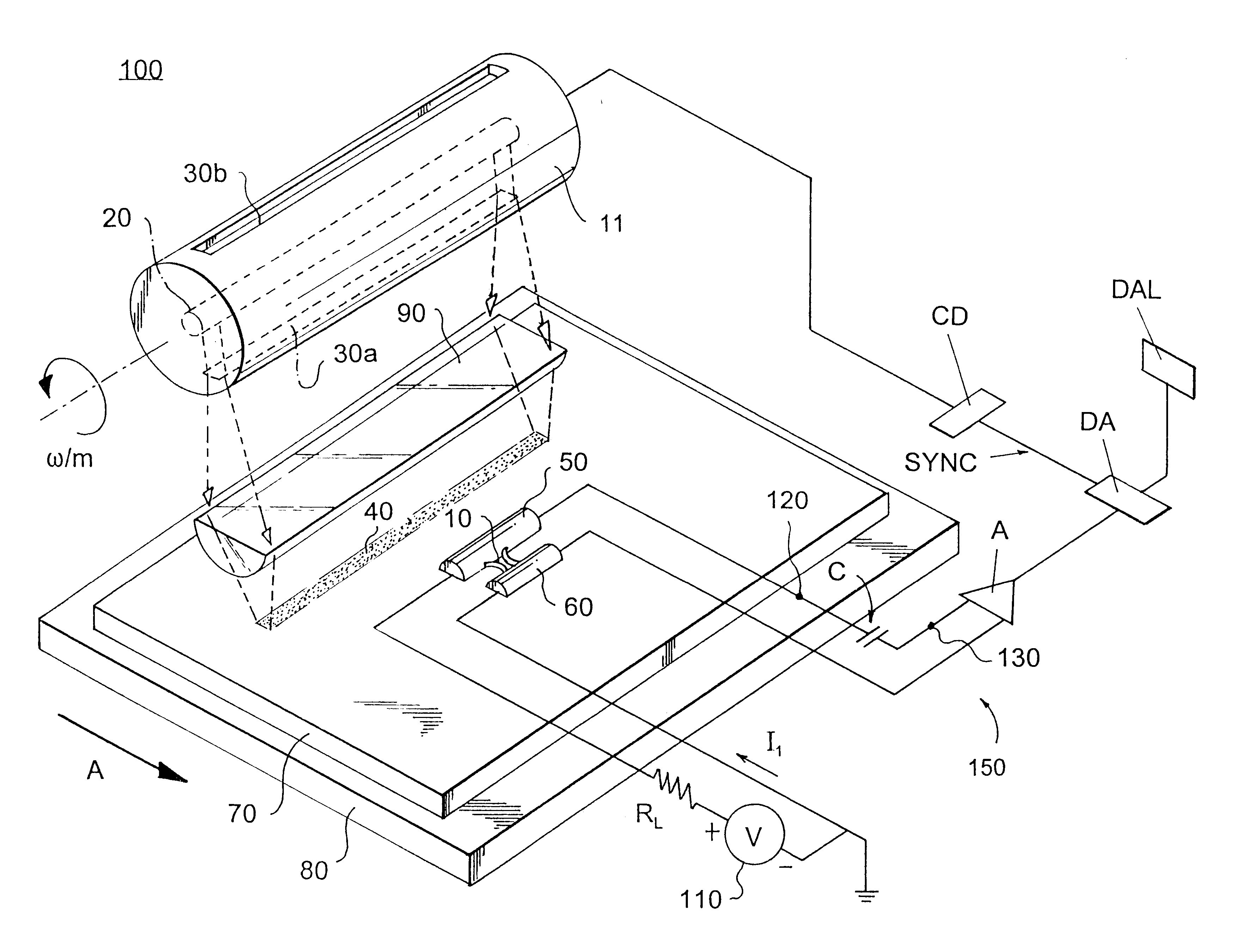
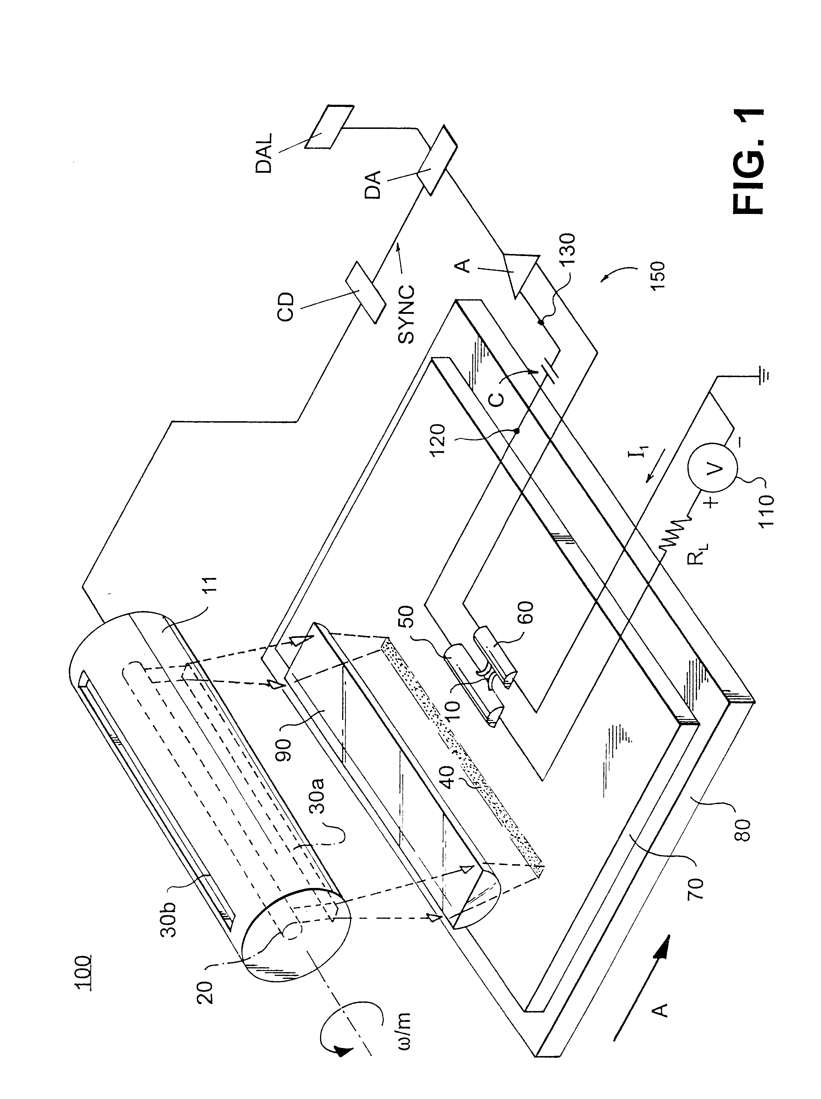
According to the invention as shown in FIG. 1, a narrow line segment 40 of incident radiant energy is applied over the entire length of a work piece at the same time and provides periodic heating over its entire length. When the thermal stimulus line segment overlaps with a circuit defect, somewhere in the workpiece, the circuit defect is periodically heated and the corresponding resistance change is measured and recorded. A long, narrow pattern of thermal stimulation reduces the time required to probe the entire workpiece, as will hereinafter be described in greater detail.

According to a first embodiment, FIG. 1 illustrates an apparatus 100 for thermally stimulating selected subsets of work piece 70 and measuring any corresponding change in circuit resistance. As shown in FIG. 1, a linear source of constant radiant energy 20, e.g., infrared radiation, is positioned within a hollow, slotted, rotating circular cylinder 11. This cylinder has "m" slot openings, for example, slot openin...

second embodiment

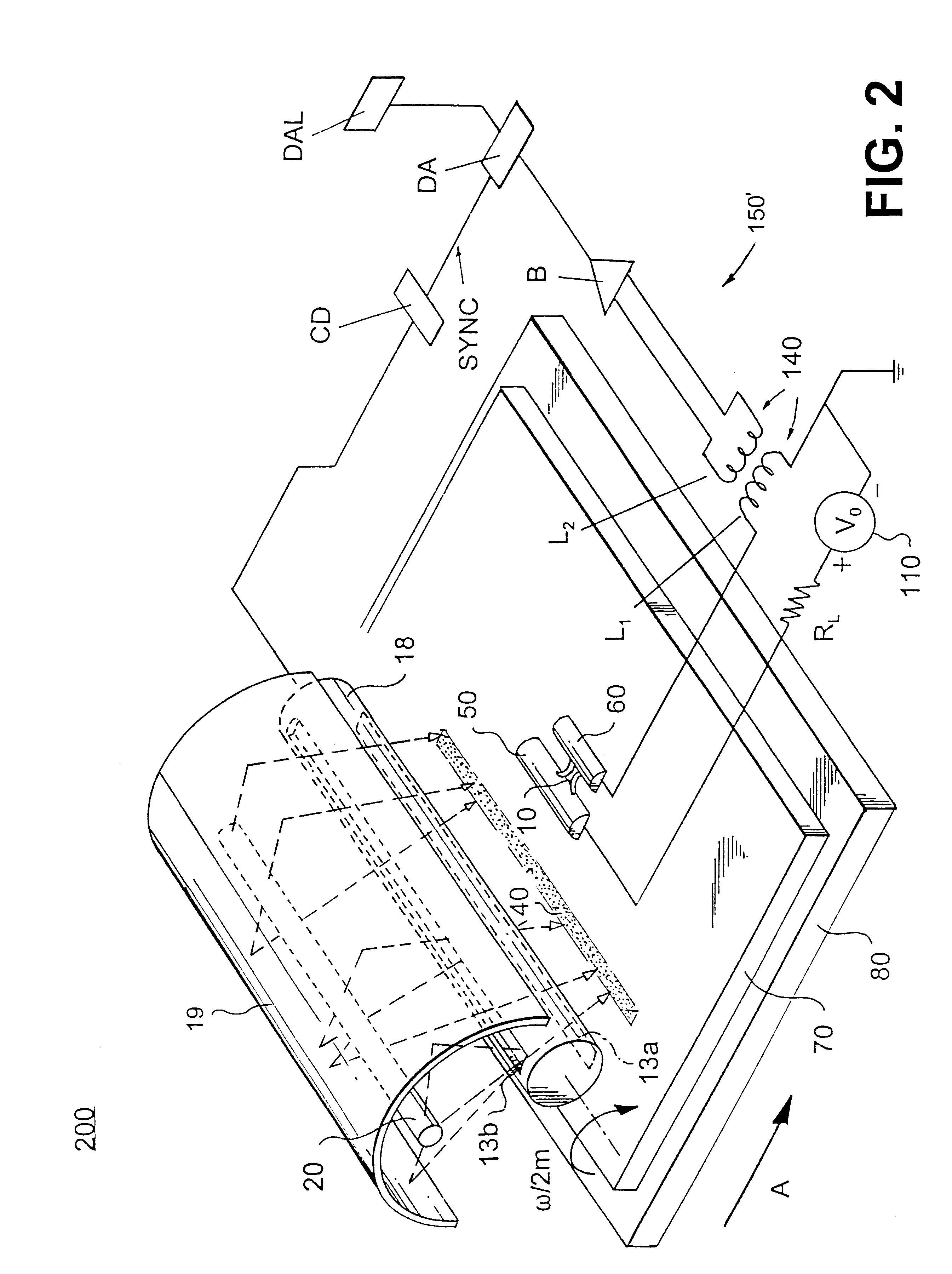
FIG. 2 illustrates an apparatus 200 according to a The apparatus of FIG. 2 operates like the apparatus 100 described with respect to FIG. 1. However, in FIG. 2, there is an elliptical trough reflector 19 which concentrates the stimulus into a narrow pattern 40. The radiation source is at one elliptical focus, and the workpiece is at the other elliptical focus. A hollow, slotted circular cylinder 18 has "m" diametrically opposed slot openings indicated as slot openings 13a, 13b, and is blocking elsewhere for radiation emanating from source 20. Preferably, the slotted circular cylinder 18 rotates at frequency .omega. / 2 m and modulates the narrow light segment 40 to turn "ON" and "OFF" at frequency .omega.. When thermal stimulus is applied to the resistive circuit defect 10, it produces a corresponding resistance change.

Procedures for locating the spatial position of resistive defect 10 are substantially as described in connection with the embodiment represented in FIG. 1.

In the detec...

embodiment 500

FIGS. 7(a)-7(d) illustrates another embodiment 500 for expediently locating a circuit defect in two resolution stages. In FIG. 7(a), the thermal stimulus pattern 440 is a rectangle, e.g., 16 mm wide by 128 mm in height, and is scanned across workpiece at eight (8) positions, labeled X1.1 thru X1.8. Suppose the corresponding measurements indicate a defect only in subset X1.4. Then in FIG. 7(b), the thermal stimulus pattern 440' is a rectangle, e.g., 128 mm wide by 16 mm in height, which is additionally applied at eight (8) positions, labeled Y1.1 thru Y1.8. Suppose the corresponding measurements indicate the defect is in subset Y1.7. Thus, the workpiece 70 circuit has a single defect, i.e., located in an area defined by the intersection of X1.4 and Y1.7, which defect is in a refined search region which covers an area 450 of about 16 mm by 16 mm, such as shown in FIG. 7(c).

In the next stage of this embodiment, the thermal stimulus pattern is a smaller rectangle 460, e.g., 16 mm in hei...


PUM

PropertyMeasurementUnit
resistanceaaaaaaaaaa
electrical resistanceaaaaaaaaaa
total resistanceaaaaaaaaaa

Abstract

A system and method for locating a circuit defect, such as a short or an incipient open, in an electric circuit in a workpiece, such a Printed Circuit Board (PCB) or MultiChip Module (MCM). The circuit is connected to a device for sensitively measuring any resistance change. A thermal stimulus is applied to various subsets of the surface of the workpiece, the thermal stimulus being temporally modulated, and the resistance change measurement correlated with this modulation. By applying well-designed thermal stimulus subsets, resistance measurements may be logically combined which correspond to the plural thermal stimulus subsets. Further, the search region where the defect may be located may be iteratively refined. By measuring the time delay between the thermal stimulus and corresponding resistance change, the depth of a defect below the surface of the workpiece is further determined. Thus the system and method efficiently and accurately locates a defect in three dimensions, even if the workpiece is large, and the defect is small and underneath the surface.

Description

1. Field of the InventionThe present invention relates generally to testing of an electric workpiece including at least one electrical circuit provided on a substrate, printed circuit board, multi-chip module, and the like, and, particularly, to a system and method employing a thermal stimulus to a circuit for efficiently and accurately locating a defect, e.g., a short circuit or an incipient open circuit, which can be practiced in the absence of a priori knowledge of circuit geometry, and which uses electrical access only at circuit terminals.2. Discussion of the Prior ArtIt is often required to fabricate an electric workpiece including one or more electrical circuits, composed of suitable electrically conducting material conduits to carry either power or signal to and from various locations in electrical circuit structures.These circuits may be either in the same plane, or may be in various planes stacked one over the other. Suitable electrical insulator materials separate these p...

Claims


Application Information

Patent Timeline
Patent Type & Authority Patents(United States)
IPC IPC(8): G01R31/08
CPCG01R31/086
Inventor GUIDOTTI, DANIELHALPERIN, ARNOLDSCAMAN, MICHAEL E.ZINGHER, ARTHUR R.
Owner GLOBALFOUNDRIES INC
Why Eureka
Try Eureka