Quantum dot infrared photodetectors (QDIP)

a quantum dot infrared and photodetecting technology, applied in the field of quantum dot infrared photodetectors, can solve the problem that normal incidence detection over a broad range in the ir can only be achieved with complicated light coupling devices and/or schemes

Inactive Publication Date: 2001-05-29
NAT RES COUNCIL OF CANADA
View PDF3 Cites 169 Cited by
  • Summary
  • Abstract
  • Description
  • Claims
  • Application Information

AI Technical Summary

Problems solved by technology

A major limitation of these QWIPs is that due to the transition selection rules they are not sensitive to normally incident light, and only have narrow response range in the IR.
Consequently, normal incidence detection over a broad range in the IR can only be achieved with complicated light coupling devices and / or schemes, and by combining layers with different sets of quantum wells each having its own narrow response range.

Method used


Image

  • Quantum dot infrared photodetectors (QDIP)
  • Quantum dot infrared photodetectors (QDIP)
  • Quantum dot infrared photodetectors (QDIP)

Examples


Embodiment Construction

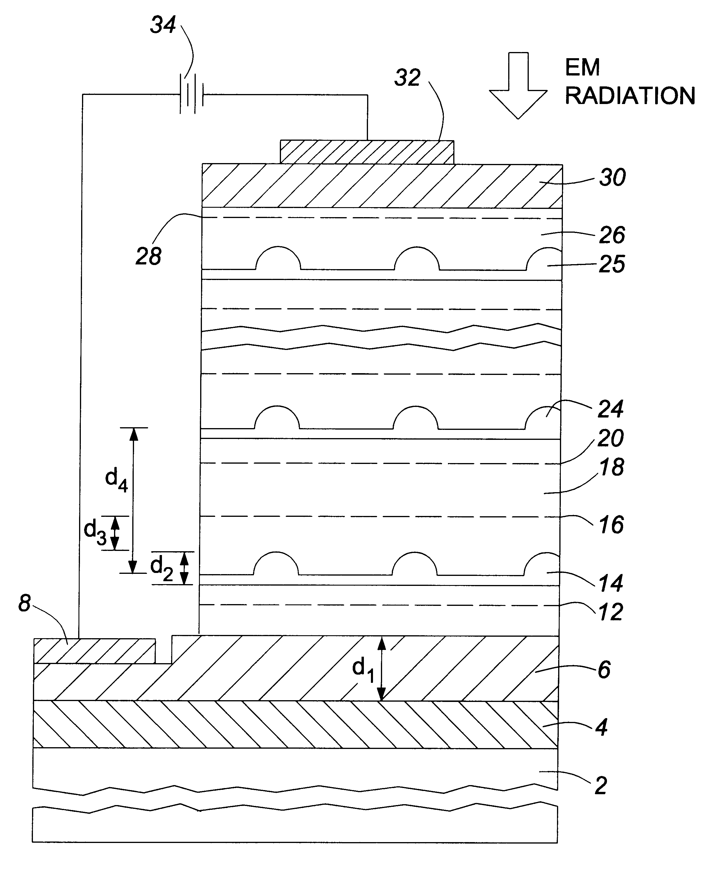
FIG. 1 illustrate a portion of the photodetector in accordance with an embodiment of the invention. The photodetector comprises multiple layers of semiconductor materials. These layers include, from bottom to top, a bottom contact layer 6 which serves as a collector or an emitter which will preferably be doped to provide carriers and for conductivity, a first barrier layer 12 which can be doped continuously or modulation doped as shown to provide carriers and for conductivity, and at least a first quantum dot layer 14.

For enhanced performance, the photodetector will preferably have multiple layers of quantum dots, in which case a barrier 18 will separate the first quantum dot layer 14 from a second quantum dot layer 24. The barrier 18 can be doped continuously or modulation doped (16 and 20) to provide carriers and for conductivity. In the case of modulation doping, multiple layers of doping can be used in the barrier 18. For example FIG. 1 illustrates the case where two modulation ...


PUM


Abstract

A photodetector capable of normal incidence detection over a broad range of long wavelength light signals to efficiently convert infrared light into electrical signals. It is capable of converting long wavelength light signals into electrical signals with direct normal incidence sensitivity without the assistance of light coupling devices or schemes. In the apparatus, stored charged carriers are ejected by photons from quantum dots, then flow over the other barrier and quantum dot layers with the help of an electric field produced with a voltage applied to the device, producing a detectable photovoltage and photocurrent. The photodetector has multiple layers of materials including at least one quantum dot layer between an emitter layer and a collector layer, with a barrier layer between the quantum dot layer and the emitter layer, and another barrier layer between the quantum dot layer and the collector.

Description

This invention relates to apparatus and methods for converting light signals into electrical signals. More particularly, the invention relates to a semiconductor photodetector device and a method for converting electromagnetic radiation such as infrared signals into electrical signals using self-assembled semiconductor quantum dots.BACKGROUND TO THE INVENTIONPresently, state-of-the art photodetectors are either based on interband transitions in bulk material or quantum wells, or intersubband transitions in quantum wells. The interband transition devices operate mainly in the visible and near infrared wavelength range due to the energy difference between the conduction and valence band of semiconductors. The intersubband devices operate with multiple layers of quantum wells, in which carriers are confined to quantum dimensions in 1 direction (perpendicular to the surface of the device), and are free to move in the other 2 directions (in the plan of the quantum wells).Such quantum wel...

Claims


Application Information

Patent Timeline
Patent Type & Authority Patents(United States)
IPC IPC(8): H01L29/06H01L31/06H01L31/0264H01L29/02H01L31/0328H01L31/102H01L31/072H01L31/0336H01L31/109H01L31/0352
CPCB82Y10/00H01L31/0352H01L31/035218H01L31/03845H01L31/09
Inventor FAFARD, SIMONLIU, HUI CHUN
Owner NAT RES COUNCIL OF CANADA
Why Eureka
Try Eureka