Multi-thickness, multi-layer green sheet processing

a green sheet, multi-layer technology, applied in the direction of chemistry apparatus and processes, other domestic objects, clayware, etc., can solve the problems of metallurgy damage, material damage in mlc lamination, and material damage in green sheets

Inactive Publication Date: 2001-07-10
IBM CORP
View PDF22 Cites 53 Cited by
  • Summary
  • Abstract
  • Description
  • Claims
  • Application Information

AI Technical Summary

Benefits of technology

It has also been found that when the multi-density multi-layer semiconductor substrate that is formed using this invention, is separated from the surfaces of the laminating plate 31, it is done without any physical or electrical or mechanical damage to any of the feature of the multi...

Problems solved by technology

This is due to a variety of reasons, such as, for example, handling, screening and stacking of green sheets thinner than 6 mils pose tremendous challenges.
However, these materials are very detrimental in MLC laminations as they melt at l...

Method used


Image

  • Multi-thickness, multi-layer green sheet processing
  • Multi-thickness, multi-layer green sheet processing
  • Multi-thickness, multi-layer green sheet processing

Examples


example 1

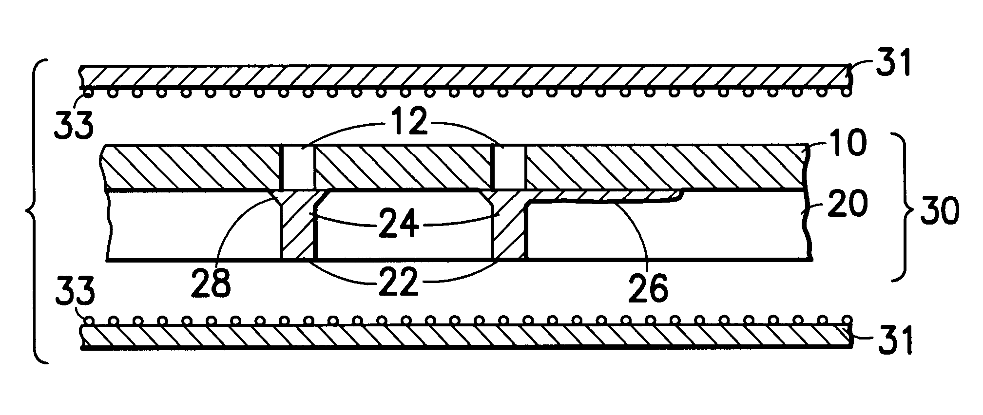
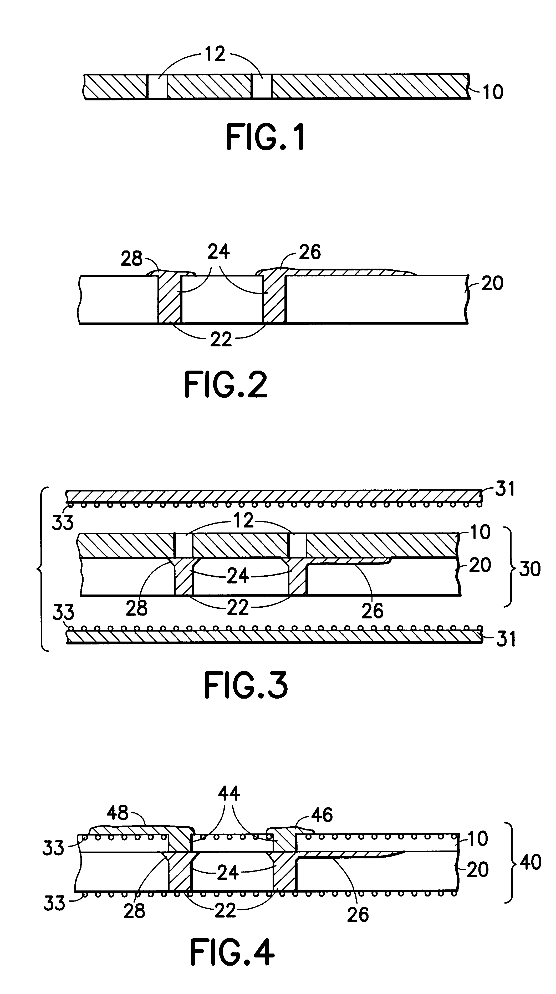
Several samples of multi-layer ceramic sub-structures containing thin green sheets 10, of thicknesses varying from about 0.8 mils to about 6.0 mils, were built on thick ceramic green sheets 20, of various thicknesses ranging from about 6 mils to about 20 mils, using the method of this invention and which resulted in a structure 30, as shown in FIG. 3. The material for the ceramic green sheets 10 and 20, included alumina and glass ceramic. The electrically conductive material included molybdenum, copper and other well-known composites. The sub-structures 30, were built at various pressures up to about 800 psi and with temperatures of up to about 90.degree. C. and by using an organic adhesion barrier material 33. In all cases the sub-structures were measured for radial error. The radial errors were found to be less than about 1.2 mils, which showed a good layer to layer contact and alignment, and no damage or distortion of the features or structure.

example 2

Several single thin ceramic green sheets 10, with thicknesses ranging from about 0.8 mils to about 3.0 mils were punched and screened as a free standing sheet 10. The material set for the green sheet 10, included alumina and glass ceramic and the electrically conductive material, included, the metal paste, such as, molybdenum, copper and other composites. In all cases the free standing screened thin ceramic layers 10, were measured for radial errors. The measured radial errors in all cases was more than about 1.2 mils and ranged up to about 15.0 mils. It was also noticed that the free-standing screened thin layers 10, were all wrinkled and non-usable.

example 3

Several samples of multi-layer ceramic sub-structures containing thin ceramic green sheets 10, of thicknesses varying from about 0.8 mils to about 6.0 mils were built with wiring density of about 3 mils on about 7 mil pitch using the method of this invention and the structure of FIG. 3, on thick green sheets 20, of various thicknesses ranging from about 6 mils to about 8 mils. The materials for the ceramic green sheets 10 and 20, included alumina and glass ceramic. The electrically conductive material included molybdenum, copper and composites. The sub-structures were built at various pressures up to about 800 psi and with temperatures up to about 90.degree. C. and by using the organic adhesion barrier materials 33. In all cases the sub-structures were measured for radial error. It was found that the radial errors were less than about 1.2 mils, which meant a good layer to layer contact and alignment. Also the substructures separated from the plates 31, with no damage to ceramic body...


PUM

PropertyMeasurementUnit
Timeaaaaaaaaaa
Thicknessaaaaaaaaaa
Thicknessaaaaaaaaaa

Abstract

The present invention relates generally to using at least one green sheet that is originally very thin with the help of at least one thicker green sheet. At least one organic adhesion barrier is used to build the multi-layer ceramic laminates. Basically, the present invention relates to a structure and method for forming laminated structures and more particularly to a structure and method for fabricating multi-density, multi-layer ceramic products using at least one very thin green sheet and/or at least one green sheet with very dense electrically conductive patterns secured to at least one thicker green sheet using at least one organic adhesion barrier.

Description

The present invention relates generally to using at least one green sheet that is originally very thin with the help of at least one thicker green sheet. At least one organic adhesion barrier is used to build the multi-layer ceramic laminates. Basically, the present invention relates to a structure and method for forming laminated structures and more particularly to a structure and method for fabricating multi-density, multi-layer ceramic products using at least one very thin green sheet and / or at least one green sheet with very dense electrically conductive patterns secured to at least one thicker green sheet using at least one organic adhesion barrier.Multi-layer ceramic (MLC) structures are used in the production of electronic substrates and devices. The MLCs can have various layering configurations. For example, a MLC circuit substrate may comprise patterned metal layers which act as electrical conductors sandwiched in between ceramic layers which act as a dielectric medium. For...

Claims


Application Information

Patent Timeline
IPC IPC(8): H01L21/48H01L21/02H05K3/46H05K1/03H01L23/12
CPCB32B37/26H01L21/481H05K3/4667B32B2315/02H05K1/0306H05K2203/068H05K2201/096H05K2203/063H05K3/4629
Inventor NATARAJAN, GOVINDARAJAN
Owner IBM CORP
Why Eureka
Try Eureka