Integrated circuit memory device incorporating a non-volatile memory array and a relatively faster access time memory cache

a non-volatile memory array and integrated circuit technology, applied in memory adressing/allocation/relocation, digital storage, instruments, etc., can solve the problems of generating more heat, providing relatively slow access times, and much more expensive production in terms of on-chip die area, so as to improve the overall access time of the page, improve the overall access time, and speed up the cycle time for read operations

Inactive Publication Date: 2001-07-17
MONTEREY RES LLC
View PDF9 Cites 55 Cited by
  • Summary
  • Abstract
  • Description
  • Claims
  • Application Information

AI Technical Summary

Benefits of technology

Disclosed herein is an integrated circuit memory device incorporating a non-volatile memory array and a relatively faster access time memory cache integrated monolithically therewith which improves the overall access time in page and provides faster cycle time for read operations. In a particular embodiment, the cache may be provided as SRAM and the non-volatile memory array provided as ferroelectric random access memory (for example, FRAM.RTM.) wherein on a read, the row is cached and the write back cycle is started allowing subsequent in page reads to occur very quickly. If in page accesses are sufficient the memory array precharge in a ferroelectric based memory array may be hidden and writes can occur utilizing write back or write through caching. In alternative embodiments, the non-volatile memory array may comprise EPROM, EEPROM or Flash memory in conjunction with an SRAM cache or a ferroelectric random access memory based cache (for example, FRAM.RTM.) which has symmetric read / write times and faster write times than EPROM, EEPROM or Flash memory.

Problems solved by technology

It does, however, provide relatively slow access times.
However, because the individual memory cell size is significantly larger, it is much more expensive to produce in terms of on-chip die area than DRAM and it also generates more heat.
While providing non-volatile data storage, their relatively slow access times (and in particular their very slow "write" times) present a significant disadvantage to their use in certain applications.
In either case, since a "read" to a ferroelectric memory is a destructive operation, the correct data is then restored to the cell during a precharge operation.

Method used


Image

  • Integrated circuit memory device incorporating a non-volatile memory array and a relatively faster access time memory cache
  • Integrated circuit memory device incorporating a non-volatile memory array and a relatively faster access time memory cache
  • Integrated circuit memory device incorporating a non-volatile memory array and a relatively faster access time memory cache

Examples


Embodiment Construction

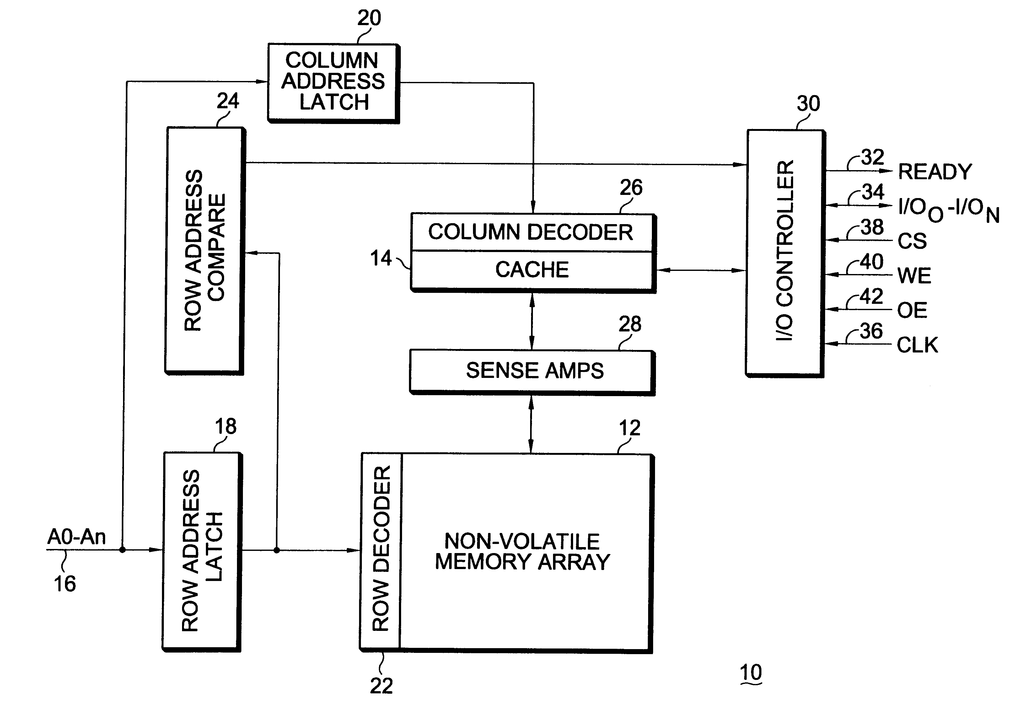
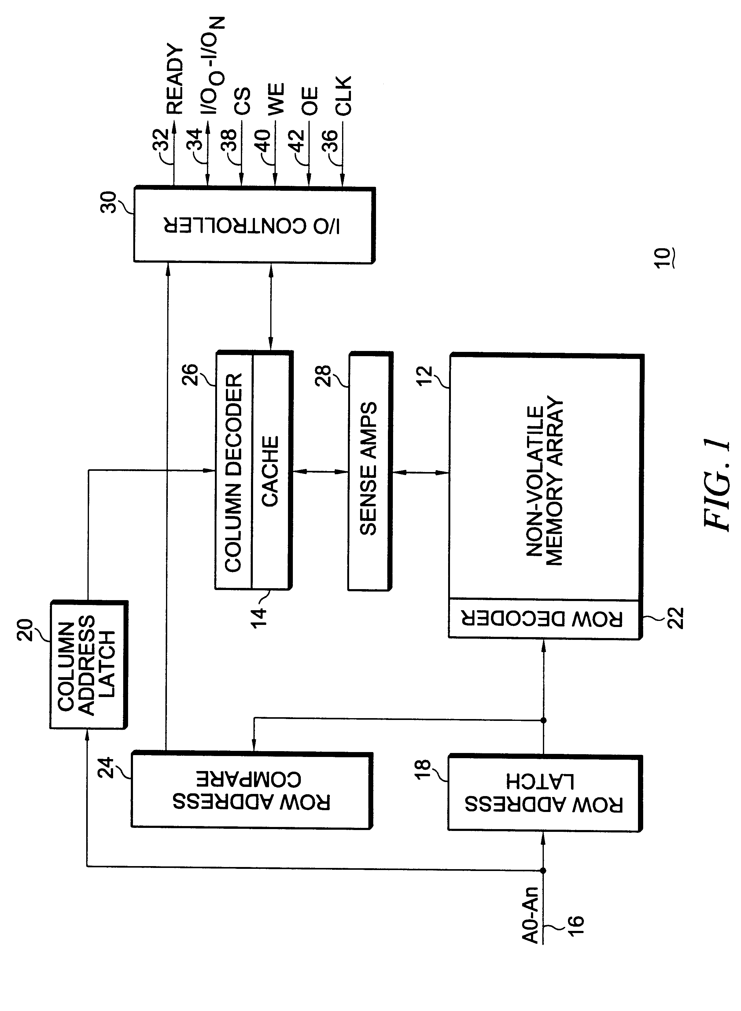
With reference now to FIG. 1, a simplified logic block diagram of a representative integrated circuit memory device 10 incorporating a non-volatile memory array 12 and a relatively faster access time memory cache 14 in accordance with the present invention is shown. It should be noted that although a parallel memory device 10 has been illustrated, the principles of the present invention are likewise applicable to those incorporating a serial data bus as well as synchronous devices.

The exemplary memory device 10 illustrated is accessed by means of an external address bus 16 comprising a number of address lines A.sub.0 through A.sub.n inclusive. The address bus is applied to a row address latch 18 as well as a column address latch 20. The row address latch 18 and column address latch 20 are operative to respectively maintain a row and column address for accesses to the non-volatile memory array 12. The output of the row address latch 18 is supplied directly to a row decoder 22 associa...


PUM


Abstract

An integrated circuit memory device incorporating a non-volatile memory array and a relatively faster access time memory cache integrated monolithically therewith improves the overall access time in page and provides faster cycle time for read operations. In a particular embodiment, the cache may be provided as static random access memory ("SRAM") and the non-volatile memory array provided as ferroelectric random access memory wherein on a read, the row is cached and the write back cycle is started allowing subsequent in page reads to occur very quickly. If in page accesses are sufficient the memory array precharge may be hidden and writes can occur utilizing write back or write through caching. In alternative embodiments, the non-volatile memory array may comprise electrically erasable read only memory ("EEPROM") or Flash memory in conjunction with an SRAM cache or a ferroelectric random access memory based cache which has symmetric read / write times and faster write times than either EEPROM or Flash memory.

Description

BACKGROUND OF THE INVENTIONThe present invention relates, in general, to the field of non-volatile integrated circuit ("IC") memory devices. More particularly, the present invention relates to an integrated circuit memory device incorporating a non-volatile memory array and a relatively faster access time memory cache integrated monolithically therewith.As the performance of computer central processing units ("CPUs") has increased dramatically in recent years, this performance improvement has far exceeded that of any corresponding increase in the performance of computer main memory. Typically, main memory has been made up of numbers of asynchronous dynamic random access memory ("DRAM") integrated circuits and it was not until the introduction of faster static random access memory ("SRAM") cache memory that the performance of systems with DRAM main memory improved. This performance improvement was achieved by making a high speed locally-accessed copy of memory available to the CPU so...

Claims


Application Information

Patent Timeline
Patent Type & Authority Patents(United States)
IPC IPC(8): G06F12/08G11C11/00G11C16/26G11C16/06
CPCG06F12/0893G11C11/005G06F2212/2022G11C16/26G06F2212/3042
Inventor TAYLOR, CRAIGCARRIGAN, DONALD G.ALWAIS, MIKE
Owner MONTEREY RES LLC
Why Eureka
Try Eureka