Method for fabricating a semiconductor structure with reduced leakage current density

a semiconductor structure and leakage current density technology, applied in the direction of gel state, crystal growth process, polycrystalline material growth, etc., can solve the problems of limiting the application of transistor films, and affecting the stability of semiconductor structures

Inactive Publication Date: 2001-08-07
APPLE INC +1
View PDF12 Cites 43 Cited by
  • Summary
  • Abstract
  • Description
  • Claims
  • Application Information

AI Technical Summary

Problems solved by technology

However, atomic level simulation of this proposed structure indicates that it likely is not stable at elevated temperatures.
), thereby limiting application for transistor films, and crystallinity was not maintained throughout the growth.
These thick buffer layers would limit the application for transistors.
Accordingly, a result is leaky films in which high electrical leakage is experienced due to oxygen deficiencies or vacancies.

Method used


Image

  • Method for fabricating a semiconductor structure with reduced leakage current density
  • Method for fabricating a semiconductor structure with reduced leakage current density
  • Method for fabricating a semiconductor structure with reduced leakage current density

Examples


Embodiment Construction

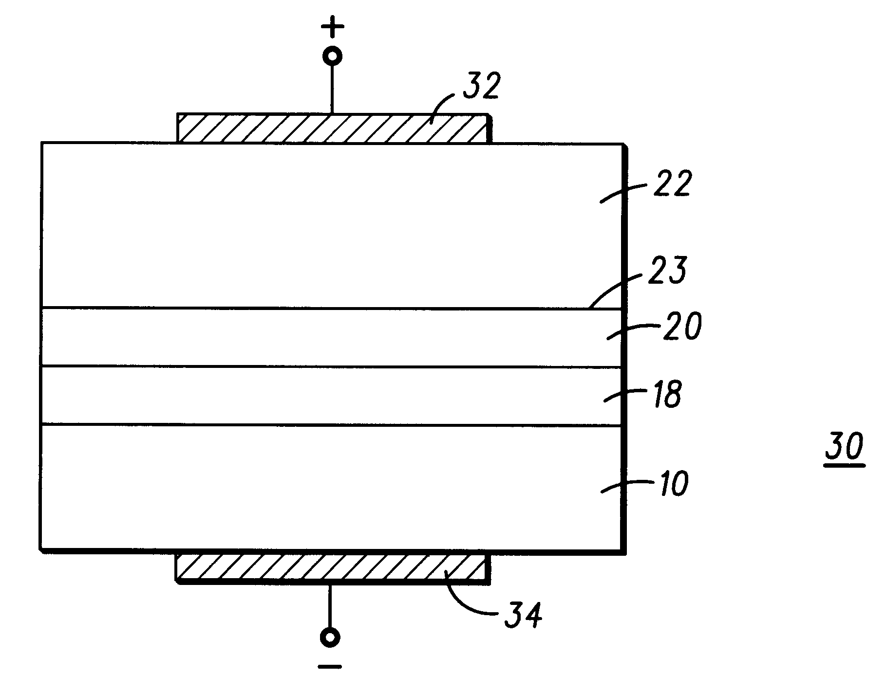
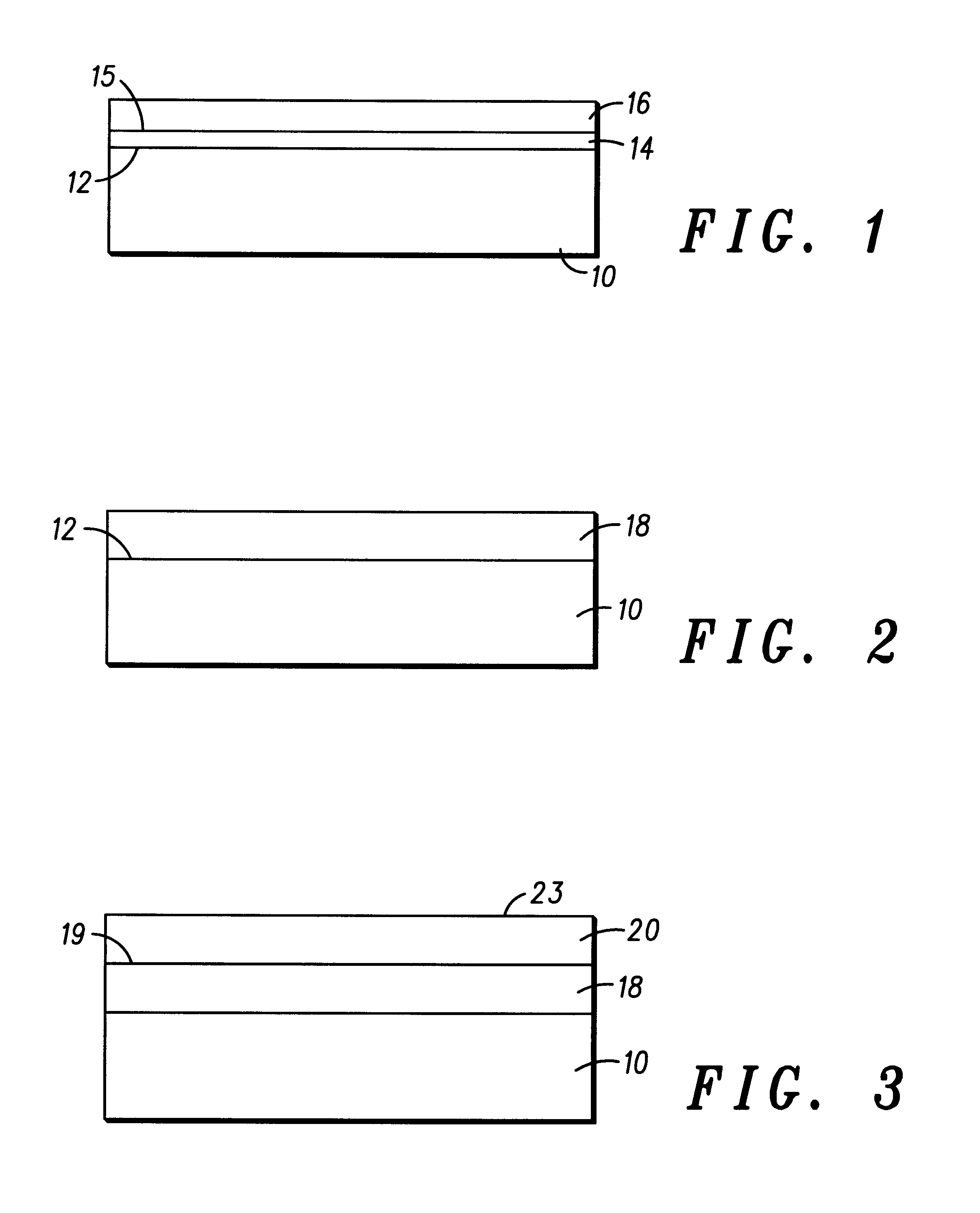
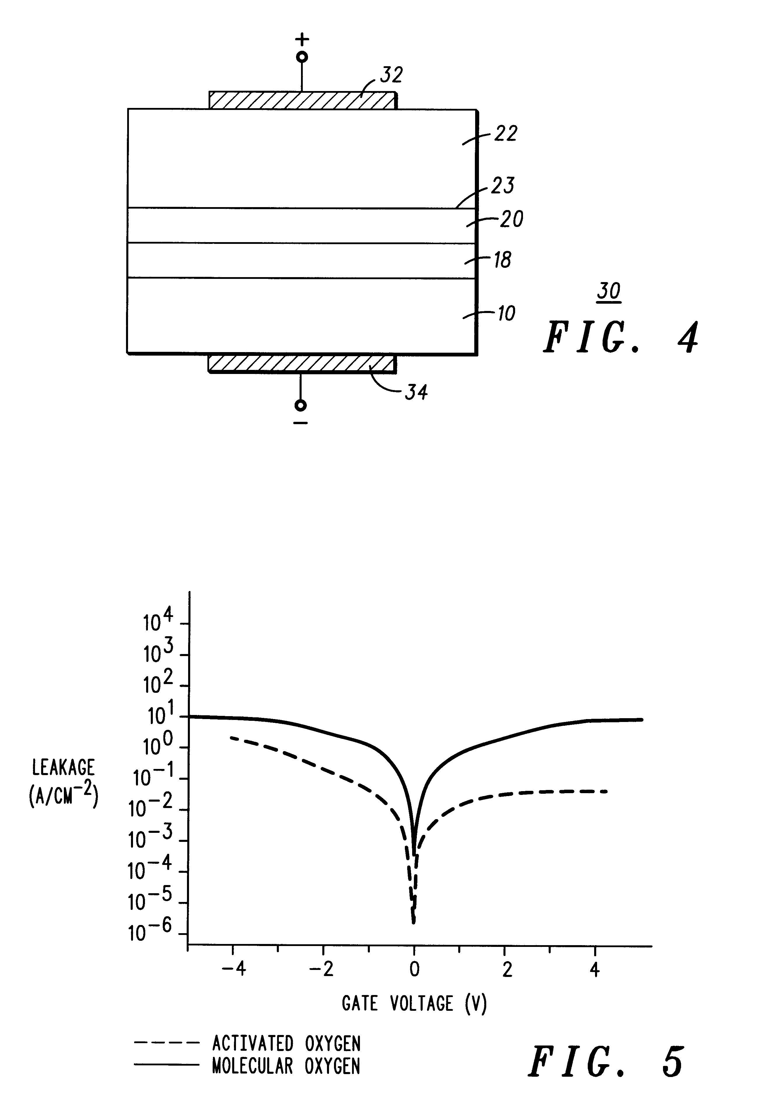
This disclosure teaches a method of fabricating a high dielectric constant (high-k) metal oxide having an interface with a silicon substrate. The process is based on the fabrication of a high dielectric constant oxide layer utilizing activated oxygen. In addition, the process includes the fabrication of a buffer layer as an interface for subsequent growth of the high dielectric constant oxide layer using molecular oxygen. Accordingly, disclosed is a new method of growing perovskite oxides such as SrTiO.sub.3, BaTiO.sub.3, SrBaTiO.sub.3, CaTiO.sub.3, or the like utilizing activated oxygen.

To form the novel interface between a silicon (Si) substrate and one or more layers of a high dielectric constant (high-k) metal oxide(s), various approaches may be used. Included are examples for starting with a Si substrate having silicon dioxide (SiO.sub.2) on the surface. The silicon dioxide is disclosed as formed of a native oxide, or utilizing thermal, or chemical techniques. SiO.sub.2 is amor...


PUM

PropertyMeasurementUnit
thicknessaaaaaaaaaa
thicknessaaaaaaaaaa
thicknessaaaaaaaaaa

Abstract

A method for fabricating a semiconductor structure including the steps of providing a silicon substrate (10) having a surface (12); forming an interface including a seed layer (18) adjacent to the surface (12) of the silicon substrate (10), forming a buffer layer (20) utilizing molecular oxygen; and forming one or more layers of a high dielectric constant oxide (22) on the buffer layer (20) utilizing activated oxygen.

Description

FIELD OF INVENTIONThe present invention relates in general to a method for fabricating a semiconductor structure including a buffer layer between a silicon substrate and metal oxides, and more particularly to a method for fabricating a semiconductor structure including a buffer layer and a high dielectric constant oxide formed using activated oxygen to reduce leakage current density.BACKGROUND OF THE INVENTIONEpitaxial growth of single crystal oxide thin films on silicon is of great interest in numerous device applications, e.g., ferroelectrics or high dielectric constant oxides for non-volatile high density memory and next generation MOS devices. Also, in the preparation of these films, it is pivotal to establish an ordered transition layer or buffer layer on the Si surface, especially for subsequent growth of single crystal oxides, e.g., perovskites.Some reported growth of these oxides, such as BaO and BaTiO.sub.3 on Si (100) were based on a BaSi.sub.2 (cubic) template by depositi...

Claims


Application Information

Patent Timeline
Patent Type & Authority Patents(United States)
IPC IPC(8): H01L21/02H01L21/316H01L21/31H01L21/8246H01L27/105
CPCH01L28/56H01L21/31691H01L21/31683H01L21/31662H01L21/02271H01L21/02266H01L21/02197H01L21/02164H01L21/31H01L21/02337
Inventor DROOPAD, RAVINDRANATHYU, ZHIYIRAMDANI, JAMAL
Owner APPLE INC
Why Eureka
Try Eureka