Structure, materials, and applications of ball grid array interconnections

a technology of grid array and interconnection, applied in the direction of dielectric characteristics, sustainable manufacturing/processing, final product manufacturing, etc., can solve the problems of difficulty in visual inspection of solder joints, cost issues of bga modules, and the inability to control the solder ball connection process, etc., to achieve stable bga joint structure, longer fatigue life, and larger module size

Inactive Publication Date: 2001-10-02
IBM CORP
View PDF47 Cites 55 Cited by
  • Summary
  • Abstract
  • Description
  • Claims
  • Application Information

AI Technical Summary

Benefits of technology

In accordance with the present invention, a strong and compliant interconnection of BGA to ceramic or plastic substrates is made possible. Moreover, the present invention makes it possible to provide a stable BGA joint structure which does not cause an excessive interdiffusion between solder balls and adjoining solder paste. Also, according to the present invention, a BGA structure which gives a longer fatigue life can be obtained. Furthermore, it is possible according to the present invention to provide a joining material and method which can handle a larger module size than that of the standard EGA module.

Problems solved by technology

The perimeter connection scheme of SMT packages has reached its limitation in terms of connection pitch and I / O capability.
A few drawbacks of BGA packages are noted such as a difficulty of visual inspection of solder joints, cost issues of BGA modules, control of solder ball connection process, lack of field reliability data, and others.
However, one major weakness of ceramic BGA is a large mismatch of thermal coefficient of expansion (TCE) between a ceramic module and a polymeric PCB.
These reactions would affect the joint integrity or degrade the long-term reliability.

Method used


Image

  • Structure, materials, and applications of ball grid array interconnections
  • Structure, materials, and applications of ball grid array interconnections
  • Structure, materials, and applications of ball grid array interconnections

Examples


Embodiment Construction

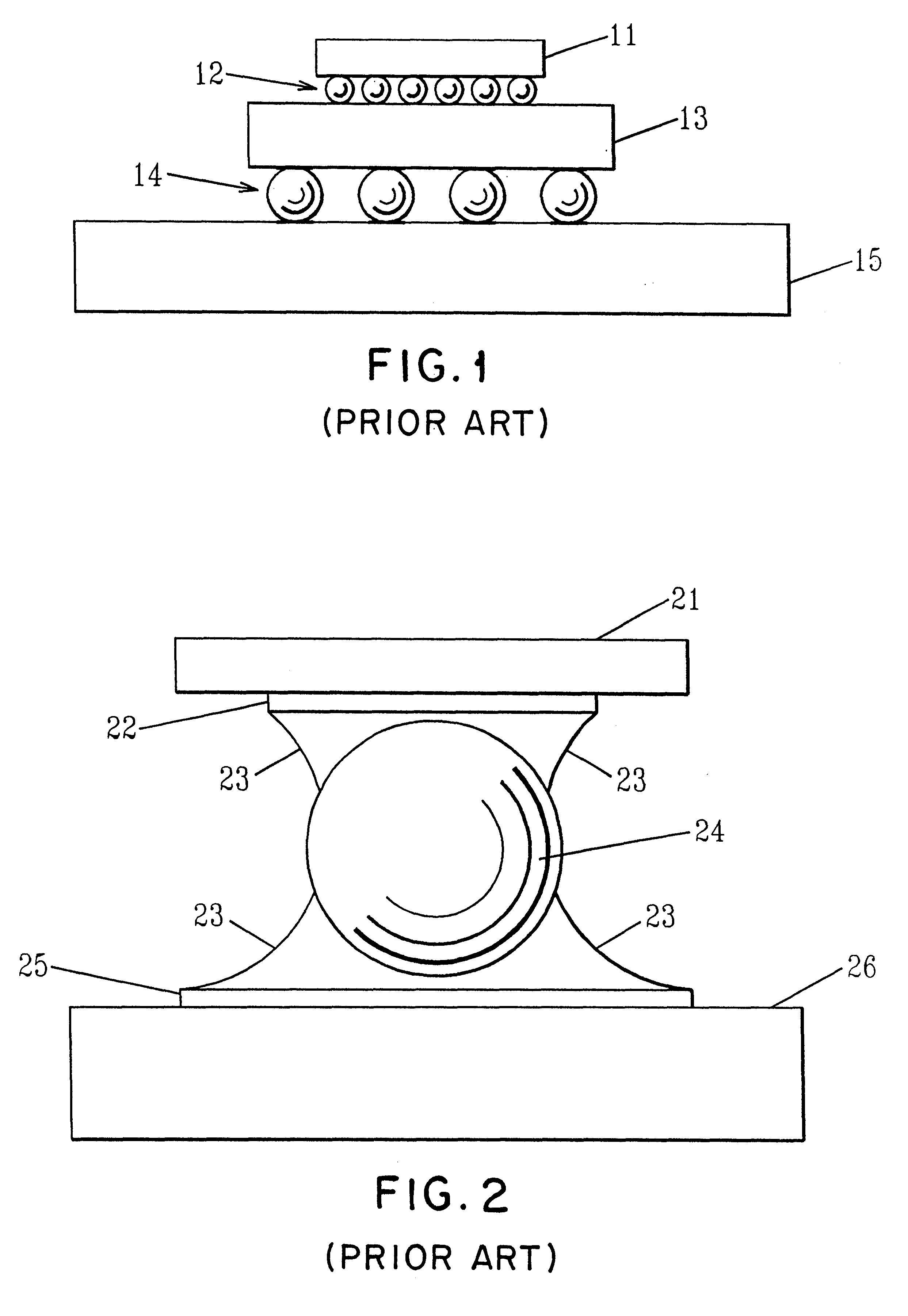
In order to facilitate an understanding of the present invention, reference will be made to the drawings.

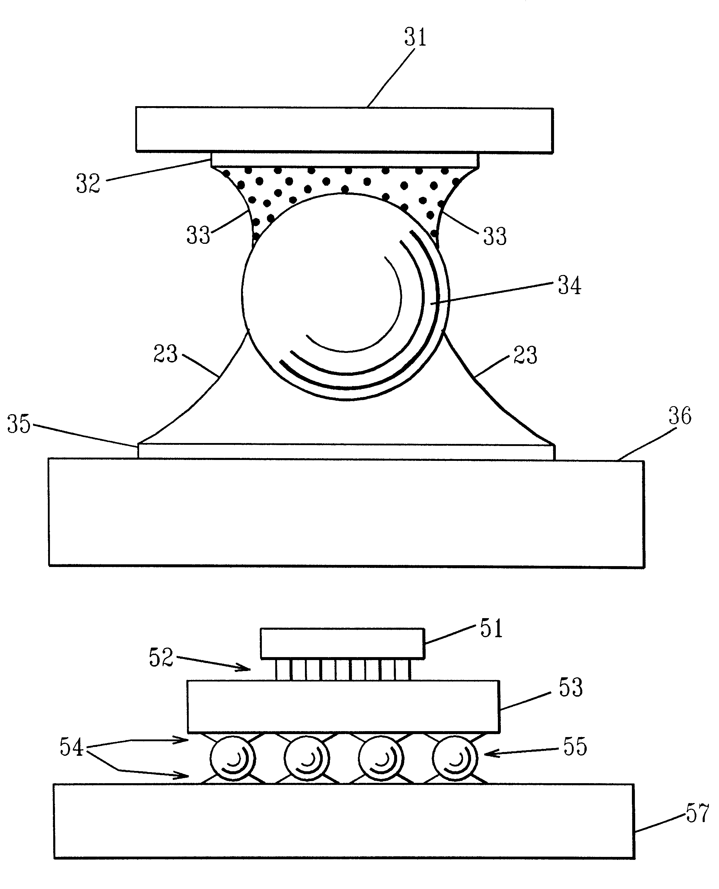
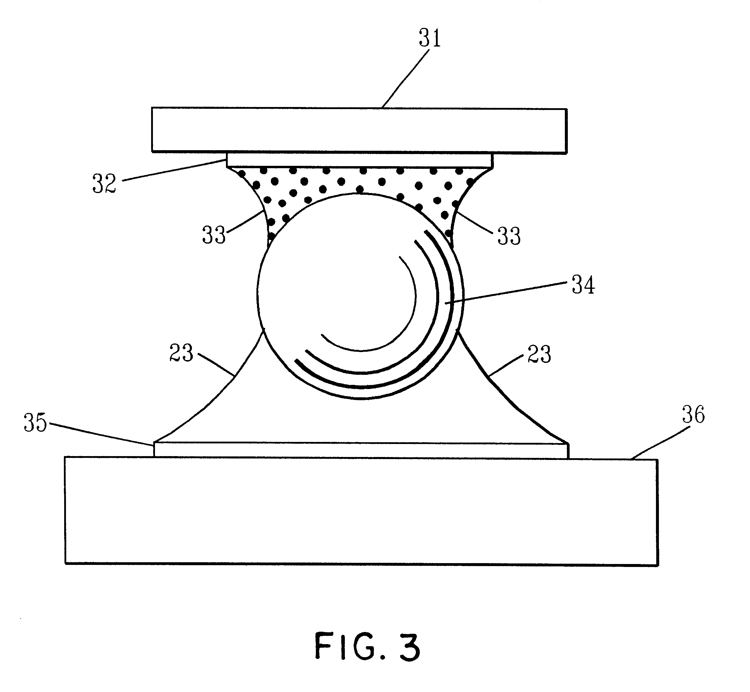
According to an embodiment of the present invention, an example of a ceramic BGA module is schematically shown in FIG. 3, where the joining of a solder ball 34 to a ceramic module 31 is accomplished by using an electrically conductive adhesive 33 and the joining of said solder ball 34 to the printed wiring board 36 is accomplished using a solder paste connection 35. The interface in the vicinity of the module is represented by 32 and that in the vicinity of the printed wiring board is represented by 23.

Examples of suitable electrically conductive adhesives 33 are disclosed in U.S. Ser. No. 08 / 641,406; U.S. Ser. No. 08 / 883,188; U.S. Ser. No. 60 / 052,172; U.S. Ser. No. 08 / 868,771 and U.S. Ser. No. 08 / 877,991, all of which are assigned to International Business Machines Corporation, the assignee of the present application, and entire disclosures of which are incorporated herein by re...


PUM

PropertyMeasurementUnit
diameteraaaaaaaaaa
thicknessaaaaaaaaaa
melting pointaaaaaaaaaa

Abstract

A new interconnection scheme of a ball grid array (BGA) module is disclosed where a solder ball is connected to the BGA module by use of an electrically conducting adhesive The electrically conducting adhesive can be a mixture comprising a polymer resin, no-clean solder flux, a plurality of electrically conducting particles with an electrically conducting fusible coating and others. The solder balls in a BGA module can also be connected to a printed circuit board by use of another electrically conductive adhesive which can be joined at a lower temperature than the first joining to the BGA module. Additionally, an electrically conducting adhesive can be formed into electrically conducting adhesive bumps which interconnect an integrated circuit device to the BGA module.

Description

The present invention relates generally to techniques for connecting an electronic device to external circuitry, and more particularly to ball grid array interconnections between microelectronic packages and printed circuit boards.BACKGROUND OF INVENTIONRapid advances in microelectronic devices are continuously demanding a finer pitch connection between electronic packages and a printed circuit board (about a few hundred micrometer pitch or less). To meet this demand as well as the demand for low cost electronic packages, surface mount technology (SMT) has expanded its share over the conventional plated-through-hole (PTH) technology for the last twenty years. At present, more than two thirds of integrated circuits (IC) including both memory and logic devices are assembled by SMT. SMT packages commonly found in a PCB are leaded chip carriers such as small outline integrated circuits (SOIC), plastic leaded chip carrier (PLCC), quad flat pack (QFP), thin small outline package (TSOP), o...

Claims


Application Information

Patent Timeline
Patent Type & Authority Patents(United States)
IPC IPC(8): H01L21/02H01L21/48H01L23/498H01L23/48H05K3/32H05K3/34
CPCH01L21/4853H01L23/49816H05K3/321H05K3/3436H05K2201/0129H05K2201/0218H05K2201/10734H05K2201/10992H05K2203/041H05K2203/0425H01L2224/16225H01L2924/15311Y02P70/50
Inventor CALL, ANSON J.DELAURENTIS, STEPHEN ANTHONYFAROOQ, SHAJIKANG, SUNG KWONPURUSHOTHAMAN, SAMPATHSTALTER, KATHLEEN ANN
Owner IBM CORP
Why Eureka
Try Eureka