Multilayered electronic part and electronic circuit module including therein the multilayered electronic part
Inactive Publication Date: 2001-10-09
TAIYO YUDEN KK
View PDF11 Cites 42 Cited by
Summary
Abstract
Description
Claims
Application Information
AI Technical Summary
This helps you quickly interpret patents by identifying the three key elements:
Problems solved by technology
Method used
Benefits of technology
Benefits of technology
It is another objection of the invention to provide an electronic circuit module with the multilayered electronic component having improved thermolytic effect, thereby facilitating the realization of the miniaturization of the electronic circuit module.
Problems solved by technology
Considering the above electronic circuit module in view of its thermal radiation, it is difficult to realize a miniaturization of the electronic circuit module.
Accordingly, if the electronic circuit module is miniaturized, it is difficult to satisfactorily getting rid of the heat induced in each components, e.g., transistor and so on.
In other words, the formation of the additional radiation fin impedes the miniaturization of the electronic circuit module and, on the other hand, the miniaturization thereof without any additional thermal radiation component will result in the insufficient thermal radiation.
Method used
Image
Click on the blue label to locate the original text in one second.
Reading with bidirectional positioning of images and text.
Examples
first embodiment
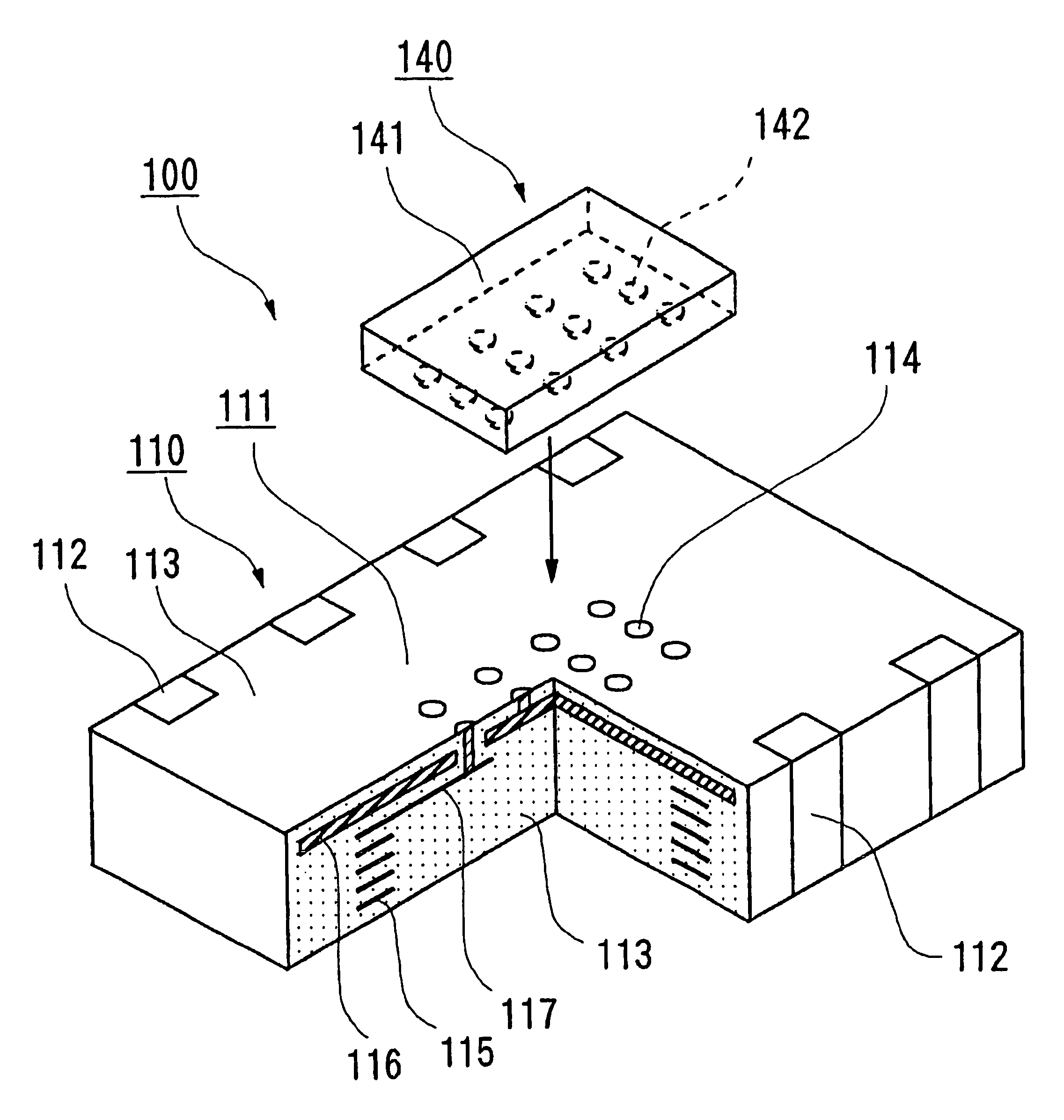
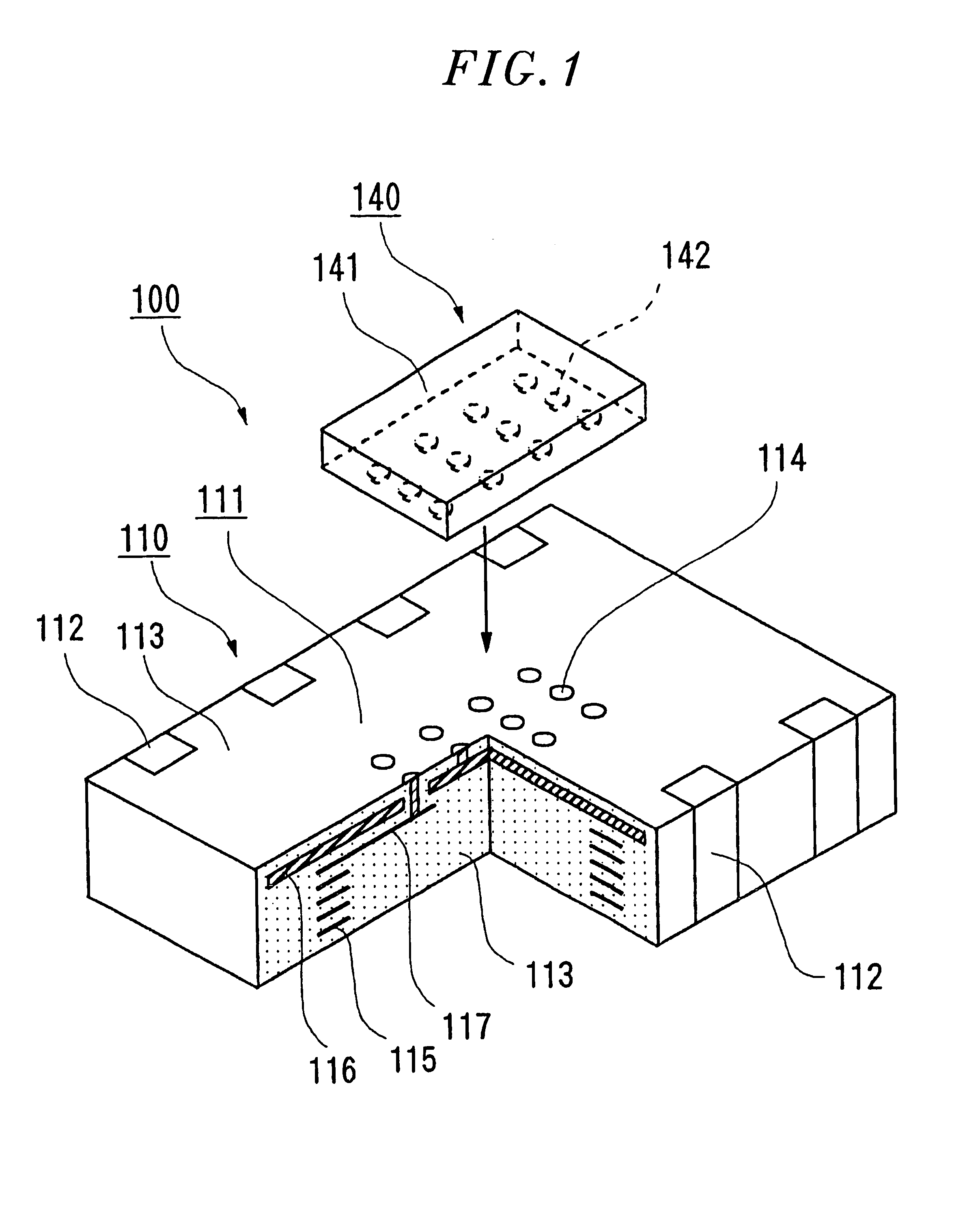
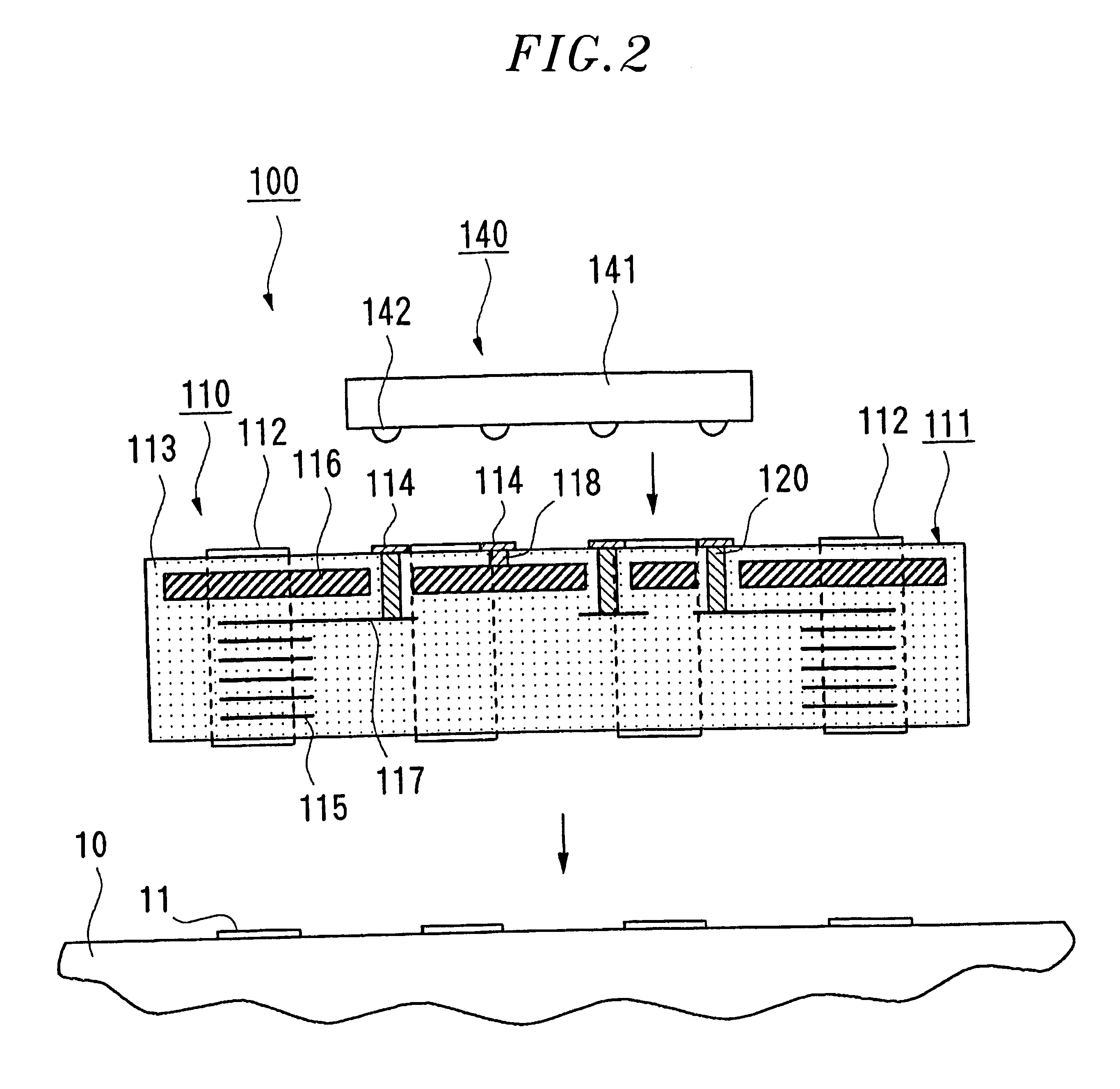
Following description with reference to FIGS. 1 to 4 is concerned with the present invention. FIGS. 1 to 4 show a fragmentary perspective view of an electronic circuit module having a partially sectioned multilayered electronic component, a cross sectional view of the electronic circuit module, a fragmentary perspective view of the multilayered electronic component, and a circuit diagram depicting an exemplary electric circuit included in the electronic circuit module, respectively.
As shown in FIG. 1, an electronic circuit module (100) is provided with a multilayered electronic component (110) having an inductor formed therein and a semiconductor chip (140). The multilayered electronic component (110) is provided with a first surface (111), a second opposite surface and side surfaces, wherein the semiconductor chip (140) is mounted on the first surface (111) and a plurality of external electrodes (112) are formed on the side surfaces. As shown in FIG. 2, the electronic circuit modul...
second embodiment
THE SECOND EMBODIMENT
Description for an electronic circuit module in accordance with the second embodiment of the present invention is followed by accompanying with FIGS. 5 to 8. FIGS. 5 to 8 show a fragmentary perspective view of the electronic circuit module having a partially sectioned multilayered electronic component, a cross sectional view of the electronic circuit module, a cross sectional view explaining the attachment between the electronic circuit module and a circuit board, and a fragmentary perspective view of the multilayered electronic component, respectively.
Differences in the electronic circuit modules between this embodiment and the first embodiment lie in a position of a semiconductor chip and a structure of external electrodes and will be described herebelow.
As shown in FIG. 5, an electronic circuit module (200) is provided with a multilayered electronic component (210) having an inductor formed therein, a semiconductor chip (240) and a plurality of metal terminal...
third embodiment
THE THIRD EMBODIMENT
Description for an electronic circuit module in accordance with the third embodiment of the present invention is followed by accompanying with FIG. 11. FIG. 11 shows a fragmentary perspective view of a multilayered electronic component in accordance with the third embodiment of the present invention.
The electronic circuit module of the third embodiment is similar to that of the first embodiment except for a structure of the multilayered electronic component. Accordingly, following description is only concerned with the multilayered electronic component of the third embodiment.
As being similar to the first embodiment, the multilayered electronic component (313) is provided with a first surface, a second opposite surface and side surfaces.
The multilayered electronic component (313) is formed by piling a plurality of magnetic green sheets (330) up, wherein each of the magnetic green sheets (330) has one of predetermined conductive patterns, as shown in FIG. 11. In d...
PUM
Abstract
The present invention provides a multilayered electronic component (110) having improved thermolytic effect for an electronic circuit module (100), facilitating the realization of a miniaturization of the electronic circuit module (100). The multilayered electronic component (110) is provided with a first surface (111), a second opposite surface and side surfaces. A heat dissipation pattern (116) is formed in the multilayered electronic component (110) in a vicinity of the first surface (111) thereof on which a plurality of lands (114) is formed, in such a way that at least one land (114) is electrically connected to the heat dissipation pattern (116). A semiconductorchip (140) is mounted on the first surface (111) of the multilayered electronic component (110), thereby forming the electronic circuit module (100). Heat induced in the semiconductorchip (140) is emitted from the heat dissipation pattern (116), which will, in turn, make a thermolytic effect of the electronic circuit module (100) be improved.
Description
The present invention relates to a multilayered electronic part or component and an electronic circuit module including therein the multilayered electronic part or component.DESCRIPTION OF THE PRIOR ARTA common electronic circuit module and a multilayered electronic component included therein have been disclosed in Japanese Laid-open Application No. 94-112090. This electronic circuit module is employed as one of function blocks such as a DC-DC converting block in such a way that a chip including an inherent electronic circuit which is formed with passive devices, e.g., resistor(s), and / or active devices, e.g., transistor(s) and IC(s), is integrated on the multilayered electronic component having a multilayered inductor and a multilayered capacitor. The multilayered electronic component has a first surface, a second opposite surface and side surfaces, wherein external electrodes are formed on the side surfaces and the chip is attached to the first surface, in such a way that when the...
Claims
Application Information
Patent Timeline
Application Date:The date an application was filed.
Publication Date:The date a patent or application was officially published.
First Publication Date:The earliest publication date of a patent with the same application number.
Issue Date:Publication date of the patent grant document.
PCT Entry Date:The Entry date of PCT National Phase.
Estimated Expiry Date:The statutory expiry date of a patent right according to the Patent Law, and it is the longest term of protection that the patent right can achieve without the termination of the patent right due to other reasons(Term extension factor has been taken into account ).
Invalid Date:Actual expiry date is based on effective date or publication date of legal transaction data of invalid patent.

