

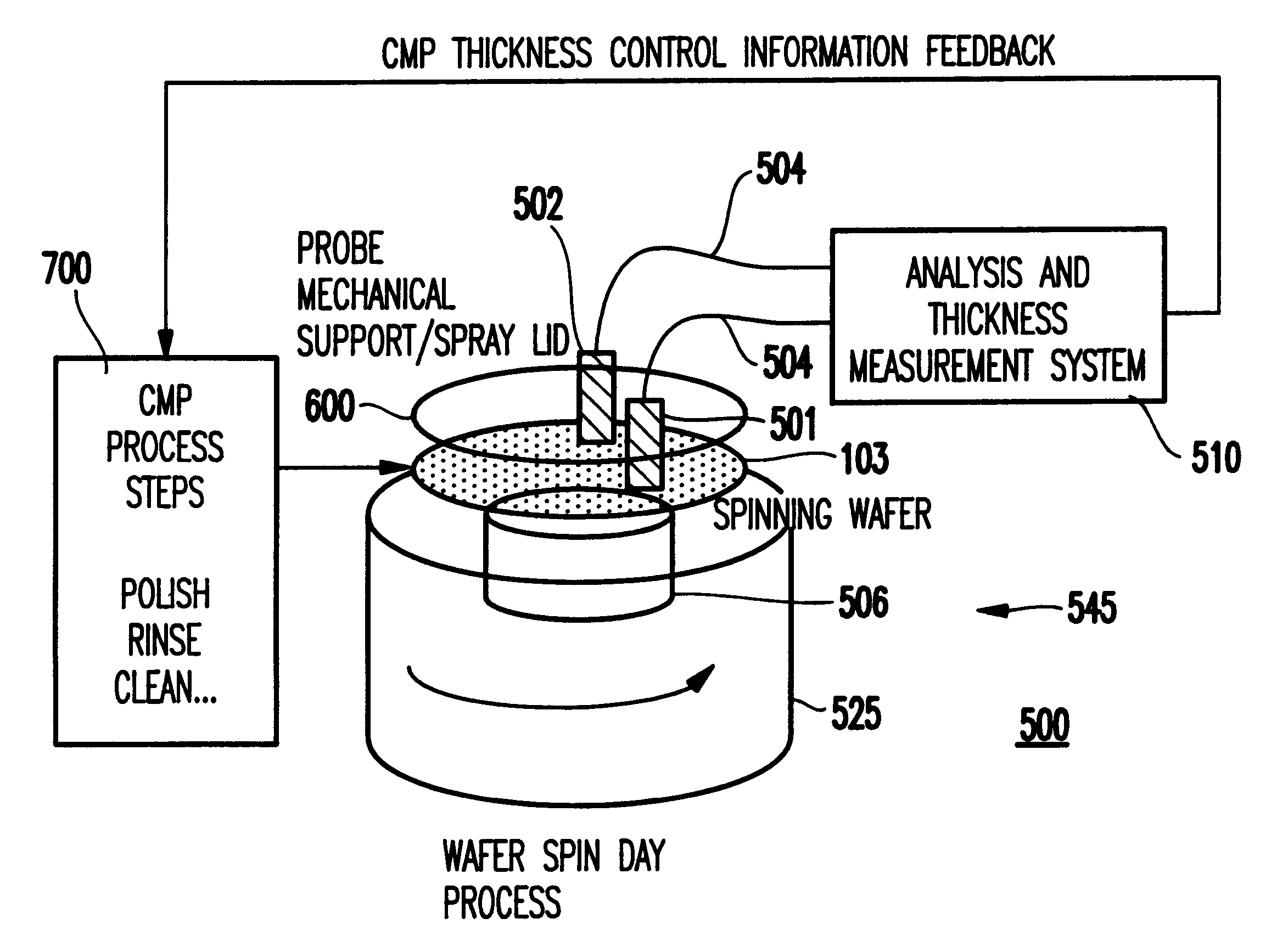
Chemical-mechanical polishing system and method for integrated spin dry-film thickness measurement
a technology of dry-film thickness measurement and chemical-mechanical polishing, which is applied in the direction of manufacturing tools, grinding machine components, lapping machines, etc., can solve the problems of slow and expensive, no effective structure or operation that minimizes the number of steps or machines, and significant delay
- Summary
- Abstract
- Description
- Claims
- Application Information
AI Technical Summary
Benefits of technology
Problems solved by technology
Method used
Image

Examples
first embodiment
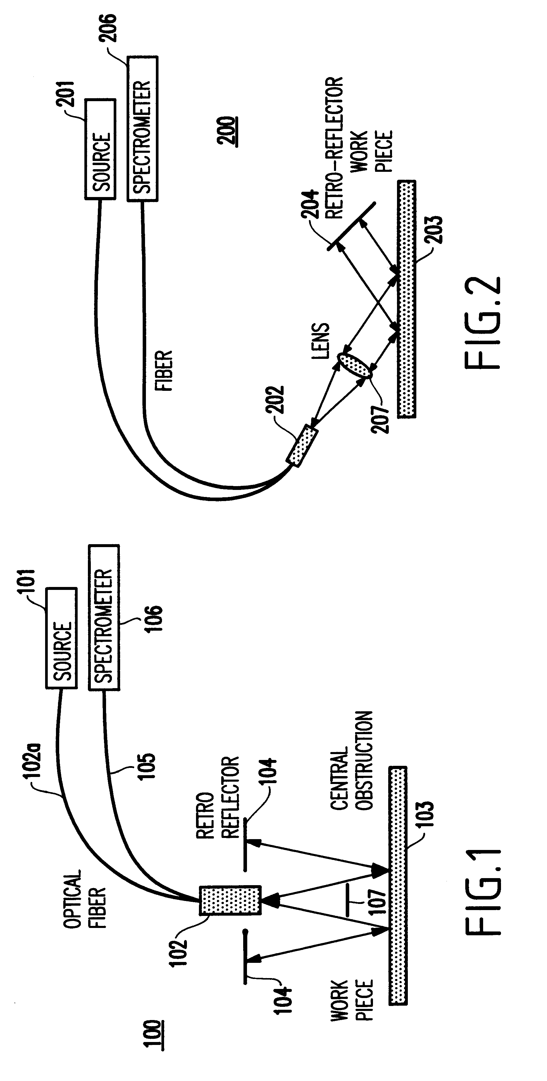
FIG. 1 illustrates the probe head design, and more specifically to a near normal incidence probe 100 that has been used in early process layers of semiconductor parts.
In FIG. 1, light is emitted from a source 101 along a fiber 102a in a cone, reflects off the wafer surface 103 under test, and retro reflects off a retro-reflector 104. The light returns to the fiber bundle 102 along the path it came through the wafer 103. A central obstruction mask 107 is placed to prevent specular (single pass) light from returning to the bundle. The light is measured by a detector 106 (e.g., a spectrometer). This first embodiment of the probe head design is the preferred form for use with the CPM system described herein. This design is especially useful in measurements of back-end oxide films. This first probe head embodiment combines ease of wafer fabrication and has excellent topography rejection.
Light that scatters from surface topography is effectively lost from the beam and does not return to t...
second embodiment
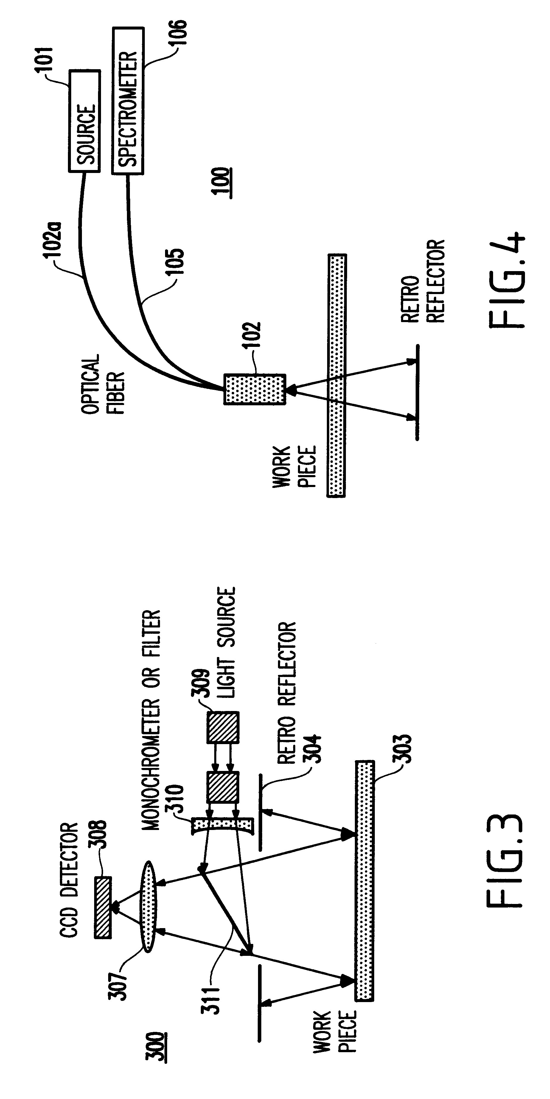
FIG. 2 illustrates a collimated beam at a large angle of incidence in a probe 200 according to the probe, having a source 201, fiber bundle 202, retroreflector 204, fiber 205, and detector 206 similar to those of FIG. 1. An objective lens 207 is provided between the fiber bundle and 202 and the wafer 203 for focusing the output from the wafer.
The probe 200 inherits the property that topography is rejected and improves overall interference signal contrast by constraining the range of angles. This range of angles may be tailored to the application (e.g., the present inventors have found + / -10 degrees or so to be useful). Small spot or narrow beam profiles can be achieved with this configuration. Both FIGS. 1 and 2 are effectively confocal in that they take light from a small aperture and return it through a small aperture. This also contributes to good interference signal contrast. In both cases, the detector 106, 206 is a spectrometer connected to the probe by a bundle of one or more...
PUM
| Property | Measurement | Unit |
|---|---|---|
| thickness | aaaaa | aaaaa |
| thickness | aaaaa | aaaaa |
| angles | aaaaa | aaaaa |
Abstract
Description
Claims
Application Information