Optoelectronic device encapsulant

a technology of optoelectronic devices and encapsulants, which is applied in the direction of optical waveguide light guides, instruments, optics, etc., can solve the problems of uncontrollable radiation, unacceptable cable size and connector size of copper wire technology, and easy to pick up radio frequency signals. , to achieve the effect of avoiding abrasion and preventing interfering accumulation

Inactive Publication Date: 2002-03-12
IBM CORP
View PDF12 Cites 54 Cited by
  • Summary
  • Abstract
  • Description
  • Claims
  • Application Information

AI Technical Summary

Benefits of technology

According to the present invention, an optoelectronic package is provided including a substrate having an array of one or more sources or detectors for generating or receiving a light signal, respectively, an optical coupler aligned with the array, and an optically transparent substrate encapsulant in contact with the substrate that substantially fills a gap between the substrate and optical coupler. The encapsulant provides the advantage of both passivating the sources or detectors and preventing interfering accumulations of matter from forming in the gap without degradation of the light signal. By way of example, the encapsulant may exhibit optical transparency to light having a wavelength of about 850 nanometers with substantially no Mie scattering. Further, the encapsulant is particularly suitable in an optoelectronic package wherein the sources are vertical cavity surface committing lasers (VCSELs). The encapsulant may also provide the advantage of further sealing wire bonds from the substrate to a cable header to avoid abrasive wear.

Problems solved by technology

Nevertheless, several disadvantages exist with current high speed copper wire cables that are driving a transition away from copper wires to fiber optic technology.
First, it is desirable to provide a large number of parallel conductors within a cable for certain applications, but the size of cables and connectors in copper wire technology are becoming unacceptably large.
Second, copper wire cables radiate radio frequency power and the radiation can be difficult to control during high speed data transmission.
Further, such cables are also susceptible to picking up radio frequency signals from external noise sources that are difficult to minimize.
Third, high speed copper wire cables are rather costly, thus, providing a cable of sufficient length for applications currently contemplated can be cost prohibitive.
Nevertheless, challenges have been encountered with incorporating VCSEL technology into parallel optoelectronic packages.
Such a gap is sufficiently large to allow extraneous debris or subsequent process chemicals to enter the gap, resulting in interfering accumulations of matter forming in the gap.
It is a disadvantage that a gap exists between the VCSEL array and optical coupler since degradation of light signals occurs as a result of accumulations in the gap.

Method used


Image

  • Optoelectronic device encapsulant
  • Optoelectronic device encapsulant
  • Optoelectronic device encapsulant

Examples


Embodiment Construction

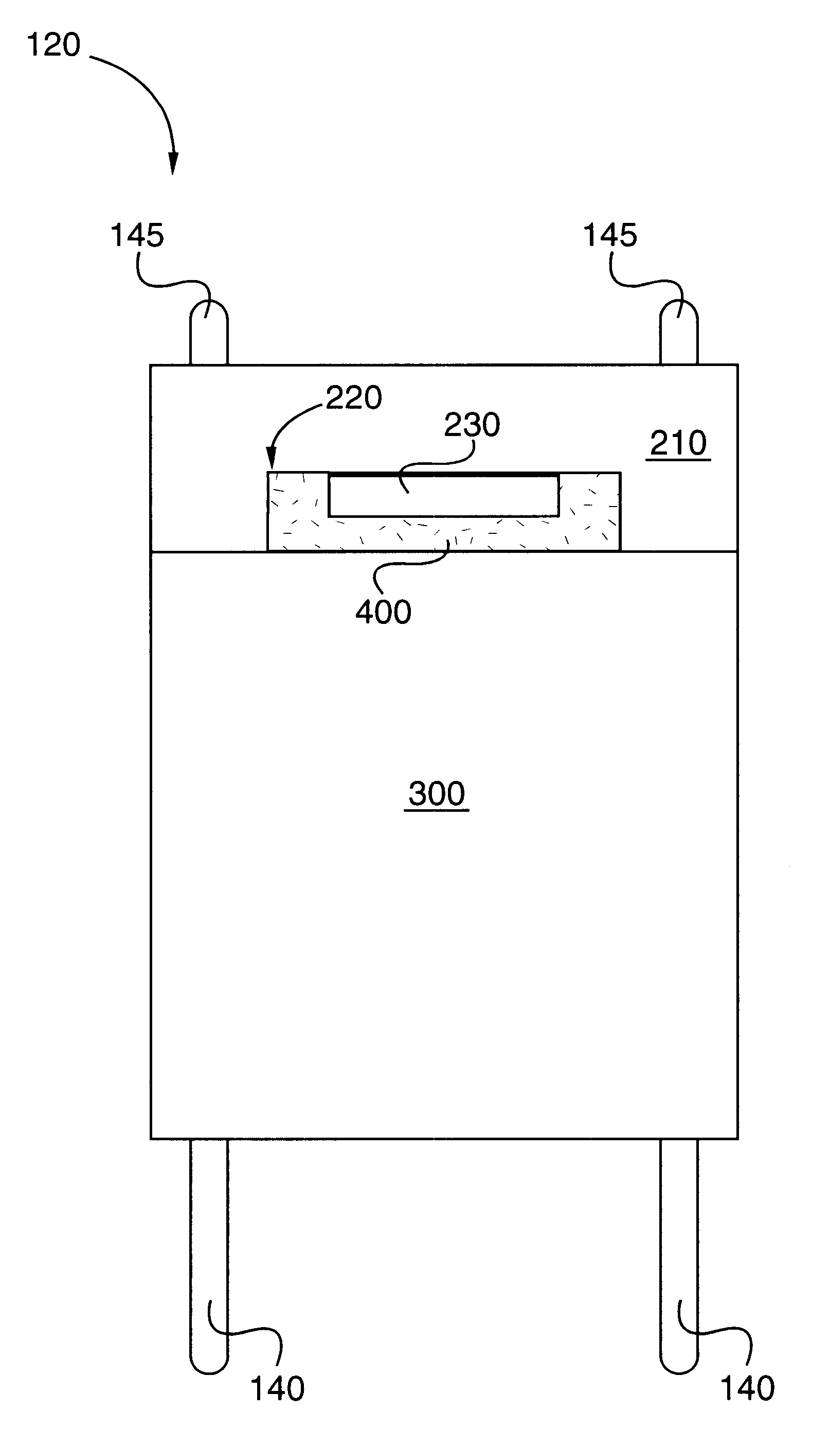
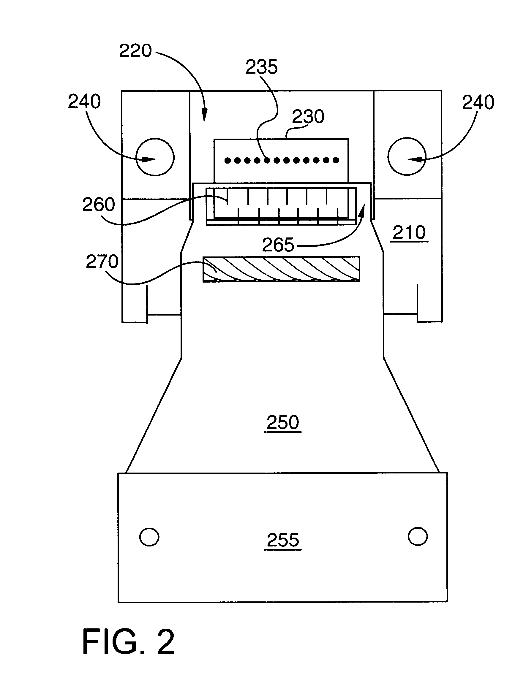
According to a preferred embodiment of the present invention, an optically clear encapsulant exhibiting a suitably high viscosity has been discovered that may be combined with a photo initiator both to replace a silicon nitride passivation layer required on a VCSEL die and to fill the gap between the die and an optical coupler, preventing light signal degradation. Thus, an optoelectronic package is provided that includes a substrate having an array of one or more sources or detectors, the sources or detectors adapted, respectively, to generate or receive a light signal, an optical coupler aligned with the array, and an optically transparent substrate encapsulant in contact with the substrate that substantially fills a gap between the substrate and optical coupler. Due to the properties of the encapsulant, it both passivates the sources or detectors and prevents interfering accumulations of matter from forming in the gap without degradation of the light signal. Preferably, the encaps...


PUM


Abstract

An optically clear encapsulant for optoelectronic packages exhibits a suitably high viscosity both to replace a silicon nitride passivation layer required on a VCSEL die and to fill a gap between the die and an optical coupler, preventing light signal degradation. The encapsulant exhibits optical transparency to light having a wavelength of about 850 nanometers (nm) with substantially no Mie scattering since particulate fillers are not required to modulate viscosity in the encapsulant. Also, the encapsulant further seals wire bonds between the die and a cable header to prevent abrasive wear. The gap-filling encapsulant is particularly suitable for use with vertical cavity surface emitting laser (VCSEL) technology. The encapsulant includes prior to curing, a difunctional acrylate epoxy resin exhibiting pseudoplastic flow and a viscosity of greater than about 0.7x10⁶ centipoise. Accordingly, a method of manufacturing an optical subassembly may eliminate a separate passivation step and instead fill the gap between the die and optical coupler with an optically clear encapsulant.

Description

1. Technical FieldThis invention relates generally to the field of optoelectronic device manufacturing and, more specifically, to encapsulants for optoelectronic devices, such as vertical cavity surface emitting laser (VCSEL) devices.2. Background ArtDevelopment of improved fiber optic data interconnects has been a goal within the optoelectronics industry. The need for increasing the rate at which information is passed between computers or between a computer and a peripheral device has been steadily rising. In the past, high speed interconnection has been accomplished to a certain extent with copper wire cables. These cables often include multiple wires with the wires being single conductors, bundled or in a ribbon configuration, coaxial cables, etc. and may be shielded to reduce electromagnetic interference (EMI) in a variety of ways.Nevertheless, several disadvantages exist with current high speed copper wire cables that are driving a transition away from copper wires to fiber opt...

Claims


Application Information

Patent Timeline
Patent Type & Authority Patents(United States)
IPC IPC(8): G02B6/42
CPCG02B6/421G02B6/4292G02B6/4212
Inventor KUCZYNSKI, JOSEPH PAUL
Owner IBM CORP
Why Eureka
Try Eureka