Advanced cobalt silicidation with in-situ hydrogen plasma clean

Inactive Publication Date: 2002-04-02
ADVANCED MICRO DEVICES INC
View PDF27 Cites 58 Cited by
  • Summary
  • Abstract
  • Description
  • Claims
  • Application Information

AI Technical Summary

Problems solved by technology

The resistances can lead to undesirably high power consumption and heat propagation in integrated circuits.
However, conventional CoSi.sub.2 processing is not without disadvantages.
Such insulating films can interfere with the cobalt-silicon reaction and lead to variations in cobalt silicide film thickness or a complete absence of cobalt silicide in certain areas.
The sensitivity of the cobalt-silicon reaction to the presence of underlying insulating fi

Method used


Image

  • Advanced cobalt silicidation with in-situ hydrogen plasma clean
  • Advanced cobalt silicidation with in-situ hydrogen plasma clean
  • Advanced cobalt silicidation with in-situ hydrogen plasma clean

Examples


Embodiment Construction

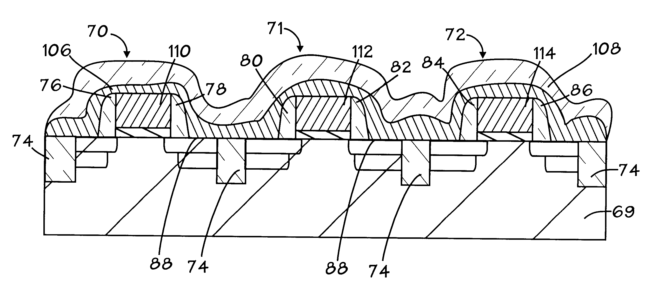
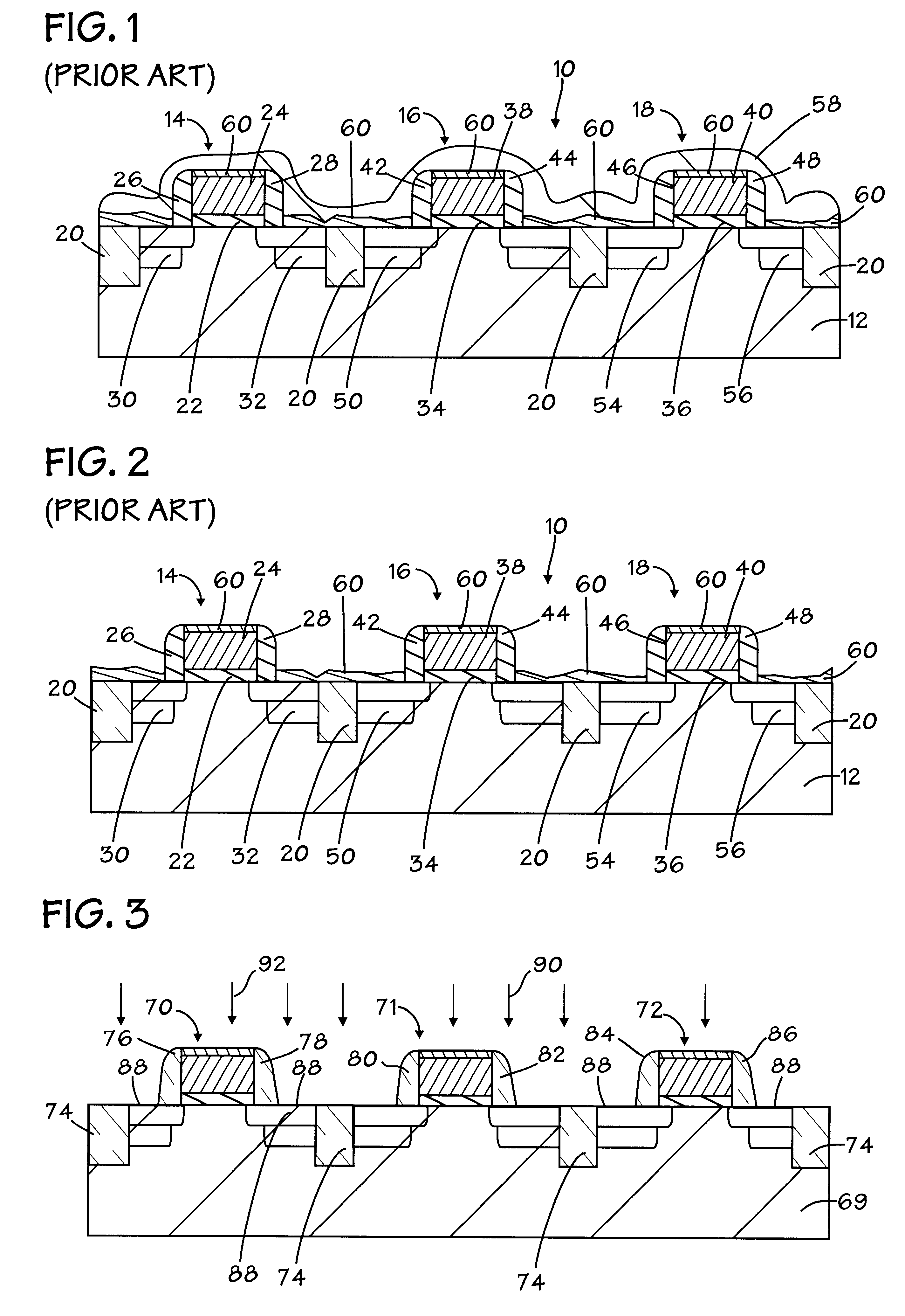
In the drawings described below, reference numerals are generally repeated where identical elements appear in more than one figure. FIGS. 1 and 2 illustrate two stages in a conventional cobalt silicide processing of an integrated circuit 10 on a semiconductor substrate 12. Only a small portion of the overall substrate 12 is illustrated in section. The integrated circuit 10 includes a plurality of circuit devices, in this case side-by-side transistors 14, 16 and 18 that are initially electrically isolated by trench isolation structures 20. The transistor 14 is depicted as a field effect transistor and consists of a gate oxide layer 22 positioned on the substrate 12 and a polysilicon gate electrode 24 positioned on the gate oxide layer 22. The gate oxide layer 22 and the gate electrode 24 are bracketed by a pair of oxide spacers 26 and 28. The transistor 14 is provided with a pair of dual graded source / drain regions 30 and 32 which are positioned in the substrate 12. The phrase "sourc...


PUM


Abstract

Various methods of fabricating a silicide structure are provided. In one aspect, a method of fabricating a circuit structure on a silicon surface is provided that includes exposing the silicon surface to a plasma ambient containing hydrogen and an inert gas, and depositing a metallic material capable of forming silicide on the silicon surface. The metallic material is heated to form a metal silicide on the silicon surface. The method provides for low sheet resistance silicide structures by eliminating native oxide films without the risk of spacer material backsputtering.

Description

1. Field of the InventionThis invention relates generally to semiconductor processing, and more particularly, to a method of fabricating a cobalt silicide film on a substrate.2. Description of the Related ArtA typical field effect transistor implemented in silicon consists of a source and a drain formed in a silicon substrate, and separated laterally to define a channel region in the substrate. A gate electrode composed of a conducting material, such as aluminum or polysilicon, is disposed over the channel region and designed to generate an electric field in the channel region. Changes in the electric field generated by the gate electrode enable, or alternatively, disable the flow of current between the source and the drain.In a conventional process flow for forming a typical field effect transistor, a gate oxide layer is grown on a lightly doped silicon substrate and a layer of polysilicon is deposited on the gate oxide layer. The polysilicon and the gate oxide are then anisotropic...

Claims


Application Information

Patent Timeline
IPC IPC(8): H01L21/306H01L21/02H01L21/285
CPCH01L21/28518H01L21/0206
Inventor FRENKEL, AUSTINSULTAN, AKIFBESSER, PAUL
Owner ADVANCED MICRO DEVICES INC
Why Eureka
Try Eureka