Method for precleaning thin film surface oxide before deposition

A surface oxide, pre-cleaning technology, used in electrical components, semiconductor/solid-state device manufacturing, circuits, etc., can solve the problems of device damage at the bottom of the contact layer, difficult to fully and effectively remove, affecting transistor performance, etc., to reduce contact resistance. Effect

Inactive Publication Date: 2009-05-27
SEMICON MFG INT (SHANGHAI) CORP
View PDF0 Cites 11 Cited by
  • Summary
  • Abstract
  • Description
  • Claims
  • Application Information

AI Technical Summary

Problems solved by technology

[0004] The existing pre-cleaning step is usually achieved by argon plasma bombardment. This physical bombardment is difficult to fully and effectively remove the natural oxide at the bottom of the contact hole and the residue formed by a series of previous processes such as wet chemical stripping, which makes the contact resistance biased. High, and the argon plasma bombardment will also cause damage to the device at the bottom of the contact layer, affecting the performance of the transistor

Method used


Image

  • Method for precleaning thin film surface oxide before deposition

Examples


Embodiment 1

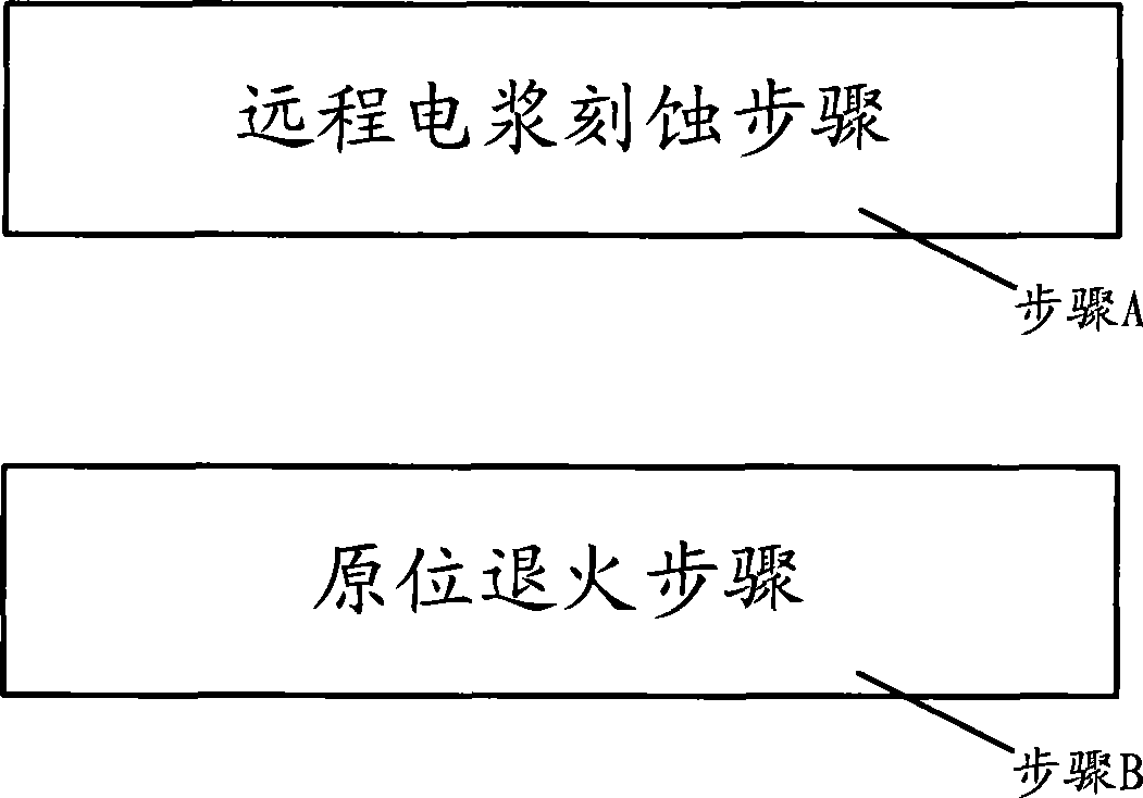
[0024] The invention introduces a method for pre-cleaning the surface oxide of the contact hole adhesion layer before deposition, the pre-cleaning method adopts a dry chemical pre-cleaning process, and mainly includes the following steps:

[0025] Step A: remote plasma etching step; etching gas includes nitrogen fluoride (NF 3 ), ammonia (NH 3 ), hydrogen (H 2 ), argon (Ar), helium (He), low-power plasma converts nitrogen fluoride and ammonia into fluorides, and fluorides react with oxides to form silicates. In this embodiment, the above-mentioned fluorides are ammonium fluoride and ammonium difluoride. Of course, the above-mentioned fluoride may be only ammonium fluoride or only ammonium difluoride.

[0026] In this step, the hydrogen in the etching gas plays a role of heat transfer in this embodiment, so that the heat transfer effect during in-situ annealing is better. The role of argon and helium is to carry the reaction gas, so that the effect of this embodiment is bet...

Embodiment 2

[0031] The difference between this embodiment and Embodiment 1 is that in this embodiment, in the remote plasma etching step of step A: the etching gas is hydrogen fluoride (HF), ammonia (NH 3 ), hydrogen (H 2 ), argon (Ar), helium (He), low-power plasma converts hydrogen fluoride and ammonia into fluoride, which reacts with oxide to form silicate.


PUM


Abstract

The invention provides a method for pre-cleaning oxide on the surface of a thin film before sedimentation. The pre-cleaning method adopts a dry-method chemical pre-cleaning process which mainly comprises the following steps: A, a remote plasma etching step: etching gas comprises nitrogen fluoride and ammonia gas; the nitrogen fluoride and ammonia gas are converted into fluoride through plasma with low power; and the fluoride reacts with the oxide on the surface of the thin film to generate silicate; and B, an in-situ annealing step: the silicate obtained in the step A is heated and sublimed to a gaseous state; and the gaseous silicate is pumped out. The disclosed method for pre-cleaning the oxide on the surface of the thin film before sedimentation adopts the dry-method chemical pre-cleaning process, can effectively clean the natural oxide of the bottom of a contact layer, can not degrade the performance of a device on the bottom layer and can simultaneously reduce the contact resistance.

Description

technical field [0001] The invention belongs to the field of chip manufacturing, and relates to a metal thin film deposition process, in particular to a method for pre-cleaning oxides on the thin film surface before deposition. Background technique [0002] The surface of a silicon wafer has multiple microchips, and each chip has millions of devices and interconnection lines, which are very sensitive to contamination. As chip feature sizes shrink to accommodate higher performance and higher levels of integration, the need to control surface contamination becomes increasingly critical. [0003] In the process before the deposition of the contact glue layer, the chip needs to be pre-cleaned to clean the natural oxide and other impurities on the surface of the film. [0004] The existing pre-cleaning step is usually achieved by argon plasma bombardment. This physical bombardment is difficult to fully and effectively remove the natural oxide at the bottom of the contact hole an...

Claims


Application Information

Patent Timeline
Patent Type & Authority Applications(China)
IPC IPC(8): C23G5/00H01L21/02
Inventor 杨瑞鹏苏娜胡宇慧陈国海保罗
Owner SEMICON MFG INT (SHANGHAI) CORP
Why Eureka
Try Eureka