Bidirectional semiconductor light-emitting element and optical system

a light-emitting element and optical system technology, applied in semiconductor laser arrangements, semiconductor lasers, lasers, etc., can solve the problems of reducing the overall power conversion efficiency, forcible power consumption, and inevitably generating electric switching losses in the installation of the rectifier circui

Inactive Publication Date: 2002-04-02
KK TOSHIBA
View PDF9 Cites 28 Cited by
  • Summary
  • Abstract
  • Description
  • Claims
  • Application Information

AI Technical Summary

Benefits of technology

According to another preferred embodiment of the invention, there may be provided an optical transmission apparatus wherein a differential wave of an electric input signal is applied to a bidirectional semiconductor light-emitting device which is capable of conducting electricity to emit light bidirectionally and which has the wavelengths of emitted lights depending on energized polarities, and an output light of the bidirectional semiconductor light-emitting device is transmitted to thereby perform signal transmission.
According to the semiconductor light-emitting element of the invention, lights can be emitted by a single device with respect to applied voltages of both positive and negative polarities, and a direct connection can be made to an AC power source to set it as an AC light emission source without using a plurality of devices or any external rectifier circuits. Accordingly...

Problems solved by technology

However, the installation of the rectifier circuit inevitably generates an electric switching loss.
Consequently, the use of the conventional semiconductor light-emitting element for an AC light source based on commercial power (AC) leads to a reduction in overall power conversion efficiency due to the loss of an external circuit even if the light conversion efficiency of the device is high.
Thus, there is a problem of forcible consumption of power corresponding to a bias current even at the non-entry time of a signal.
However, this method necessitated more than one semiconductor light-emitting elements to be provided, therefore, the whole structure become...

Method used


Image

  • Bidirectional semiconductor light-emitting element and optical system
  • Bidirectional semiconductor light-emitting element and optical system
  • Bidirectional semiconductor light-emitting element and optical system

Examples


Embodiment Construction

The present invention will be described below in detail with reference to the accompanying drawings.

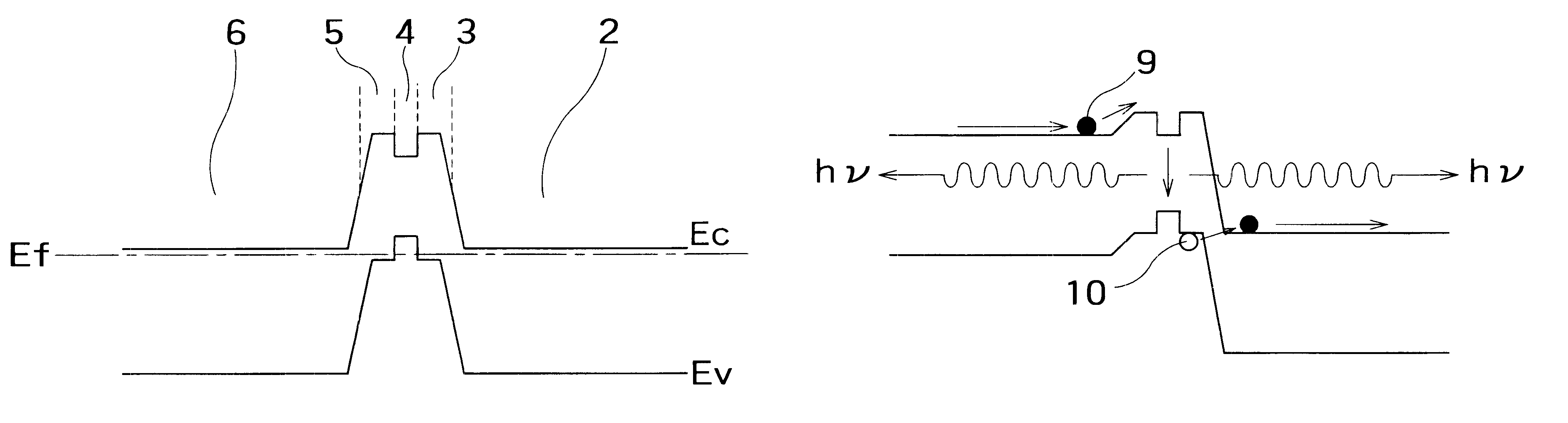
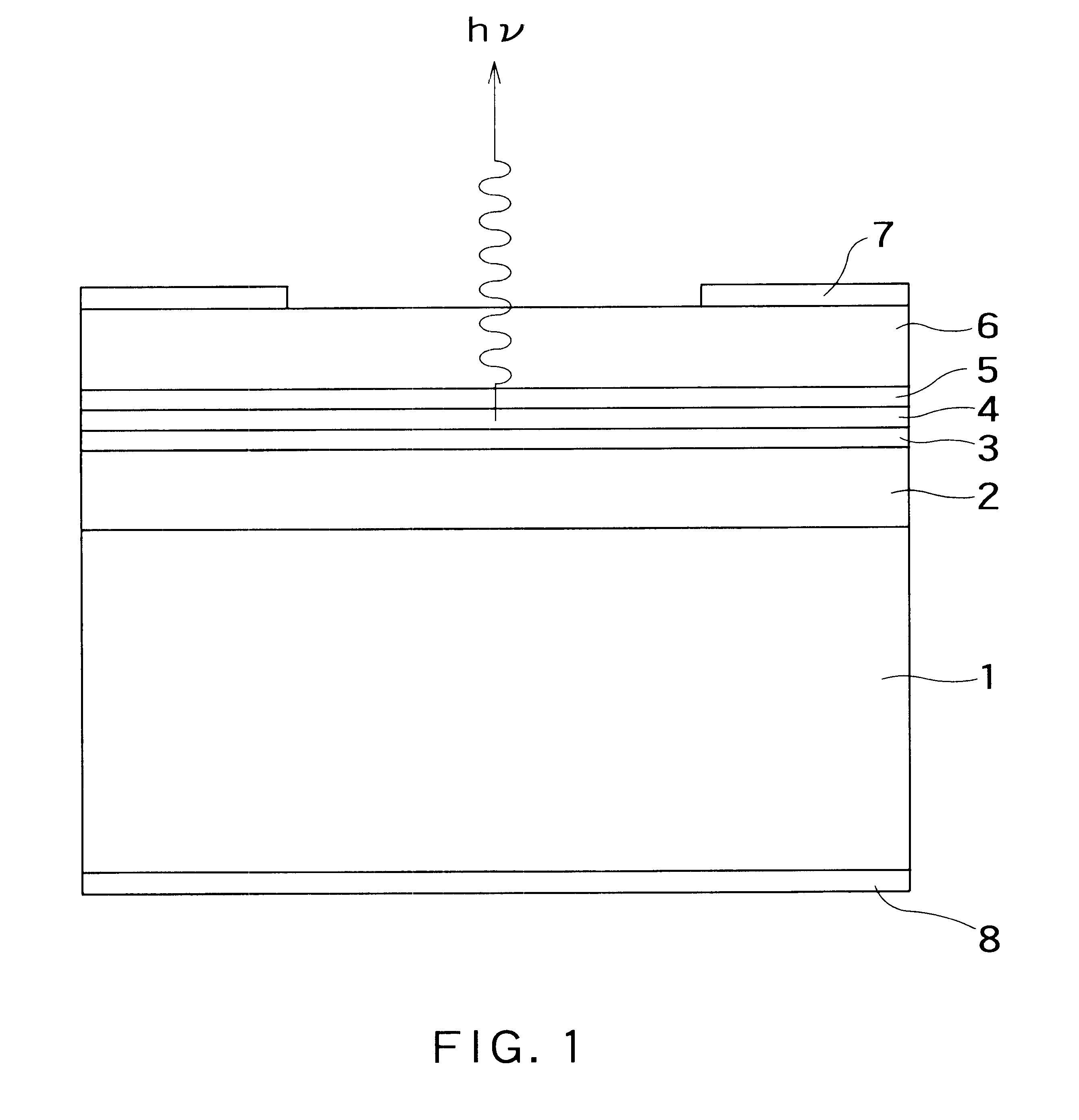
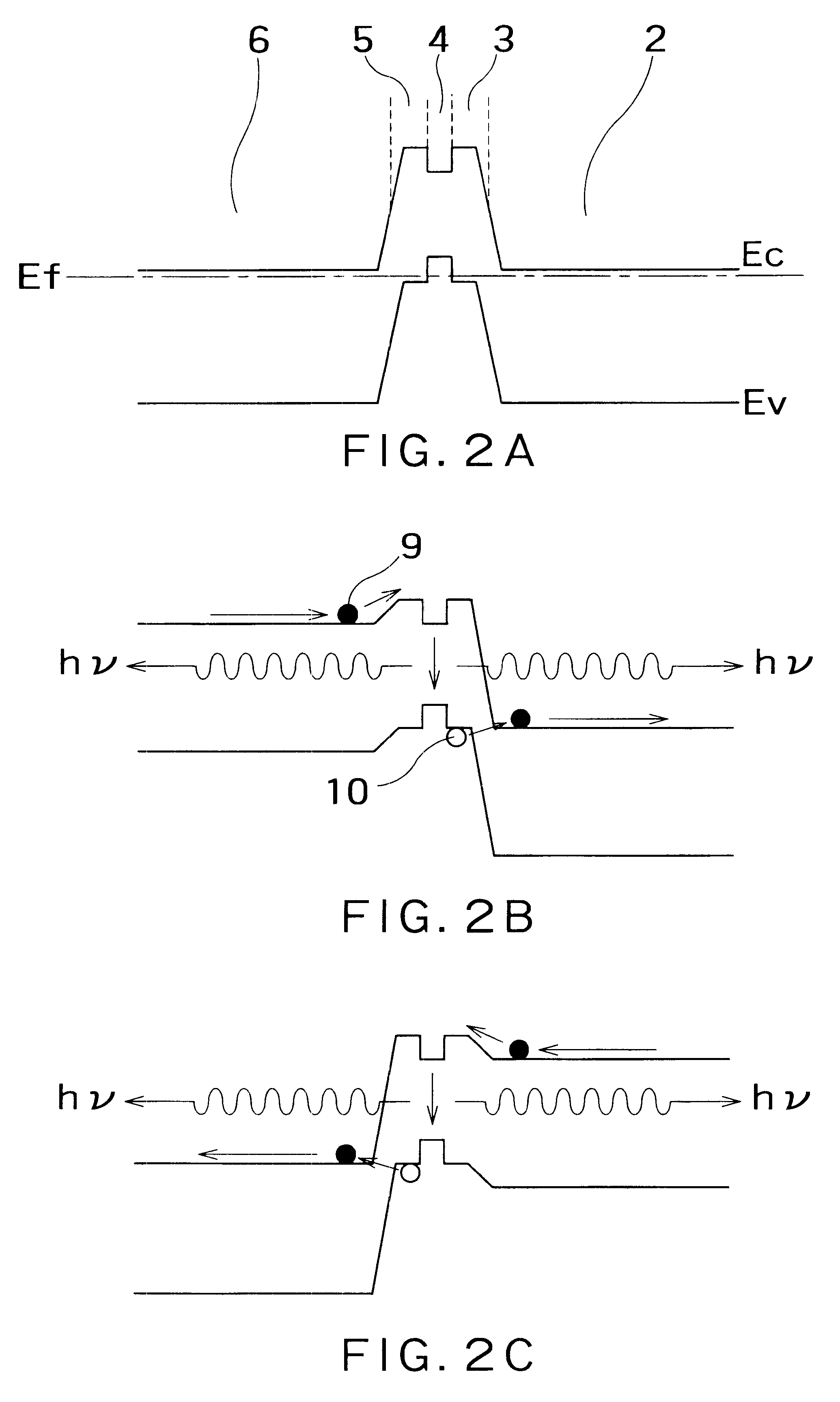
FIG. 1 schematically shows in section the structure of a bidirectional semiconductor light-emitting element according to an embodiment of the invention, by taking an example of the device of an n-p-n junction type. In the drawing, a reference numeral 1 denotes an n-type semiconductor substrate; 2 a high concentration n-type semiconductor layer; 3 a high concentration p-type semiconductor layer; 4 a light emitting layer (active layer); 5 a high concentration p-type semiconductor layer: 6 a high concentration n-type semiconductor layer; and 7 and 8 electrode metals. The p-n junction of the reference numerals 2 and 3 and the p-n junction of the reference numerals 5 and 6 exhibit usual p-n junction characteristics under a forward bias. However, these p-n junctions are set to generate a tunneling current between bands When a reverse bias of a predetermined magnitude or higher is applied.

As...


PUM


Abstract

According to the invention, a bidirectional semiconductor light emitting element is provided, which comprises: a first semiconductor region of a first type of conductivity; a second semiconductor region of a second type of conductivity provided on the first semiconductor region; a third semiconductor region of a first conductivity type provided on the second semiconductor region; and a semiconductor light emitting layer interposed in the second semiconductor region, the light emitting layer emitting light by an injection of a tunneling current generated at a reverse-biased p-n junction between the first and second regions or between the second and third regions under an application of a voltage of a first polarity across the first and third semiconductor regions, and the light emitting layer emitting light by an injection of a tunneling current generated at another reverse-biased p-n junction between the first and second regions or between the second and third regions under an application of a voltage of a second polarity, which is opposite to the first polarity, across the first and third semiconductor regions.

Description

BACKGROUND OF THE INVENTIONThe present invention relates to a bidirectional semiconductor light-emitting element capable of emitting lights irrespective of the application of a positive or negative bias voltage.A semiconductor light-emitting element such as a light-emitting diode or a semiconductor laser has characteristics including a compact form, a high efficiency, a long life and so on, and hence it has been used for various purposes as a light source in place of a conventional electric lamp or various tube lasers. However, since such a semiconductor light-emitting element basically uses a carrier injection type diode based on a p-n junction or a metal-semiconductor junction, a forward or a reverse polarity is present when a bias voltage is applied to the device. In addition, for this reason, the device generally exhibits an operational characteristic such as a half wave current-rectifying when an AC voltage is applied.Owing to such diode characteristics, it is required to insta...

Claims


Application Information

Patent Timeline
IPC IPC(8): H01L33/00H01S5/00H01S5/183H01S5/40H01S5/42H01L33/04H01L33/30H01L33/48
CPCB82Y20/00H01L33/04H01S5/18397H01S5/3095H01L33/30H01L33/06
Inventor FURUYAMA, HIDETO
Owner KK TOSHIBA
Why Eureka
Try Eureka