Method of etching silicon nitride by a mixture of CH2 F2, CH3F or CHF3 and an inert gas

a silicon nitride and inert gas technology, applied in the direction of semiconductor devices, electrical equipment, basic electric elements, etc., can solve the problems of etching selectivity of silicon nitride to silicon oxide and anisotropy trade-offs with each other, and increase the damage of silicon substrates

Inactive Publication Date: 2002-04-23
FUJITSU SEMICON LTD
View PDF11 Cites 203 Cited by
  • Summary
  • Abstract
  • Description
  • Claims
  • Application Information

AI Technical Summary

Problems solved by technology

ing. Besides, damage of the silicon substrate is increased under such SiN.sub.x etching condi
Meanwhile, followings have arisen as problems in the SAC technique.
While, followings have arisen as problems in the BLC technique.
As described above, in the above prior art, there has been such a problem that the etching selectivity of the silicon nitride to the silicon oxide and the anisotropy have trade-off relations with each other.
Hence, in the step of forming the semiconductor device employing the SAC technique, because such etching process is employed, the silicon nitride layer can be excessively etched not to remain the silicon nitride on the side surfaces of the side walls of t

Method used


Image

  • Method of etching silicon nitride by a mixture of CH2 F2, CH3F or CHF3 and an inert gas
  • Method of etching silicon nitride by a mixture of CH2 F2, CH3F or CHF3 and an inert gas
  • Method of etching silicon nitride by a mixture of CH2 F2, CH3F or CHF3 and an inert gas

Examples


second example

FIGS. 15A to 15K are sectional views showing steps of manufacturing a DRAM cell to which the above etching technique is applied.

First of all, steps of forming a configuration shown in FIG. 15A will be explained.

The field oxide film 22 is formed on the silicon substrate 21 by the selective oxidation method. The field oxide film 22 is formed to surround a device forming region A. Formation of this field oxide film 22 may be carried out according to common conditions, otherwise it may be carried out along the steps being explained in the first example. An about 60 .ANG. thick gate insulating layer 23 made of SiO.sub.2 is formed in the device forming region A.

Then, a polysilicon layer 24, a silicide layer 25, and a first cap layer 26 made of SiO.sub.2 are formed in sequence on the overall silicon substrate 21 to have thicknesses of 500 .ANG., 700 .ANG., and 800 .ANG. respectively. The silicide film 25 is made of tungsten silicide, titanium silicide, etc. and is formed by the salicide te...

third example

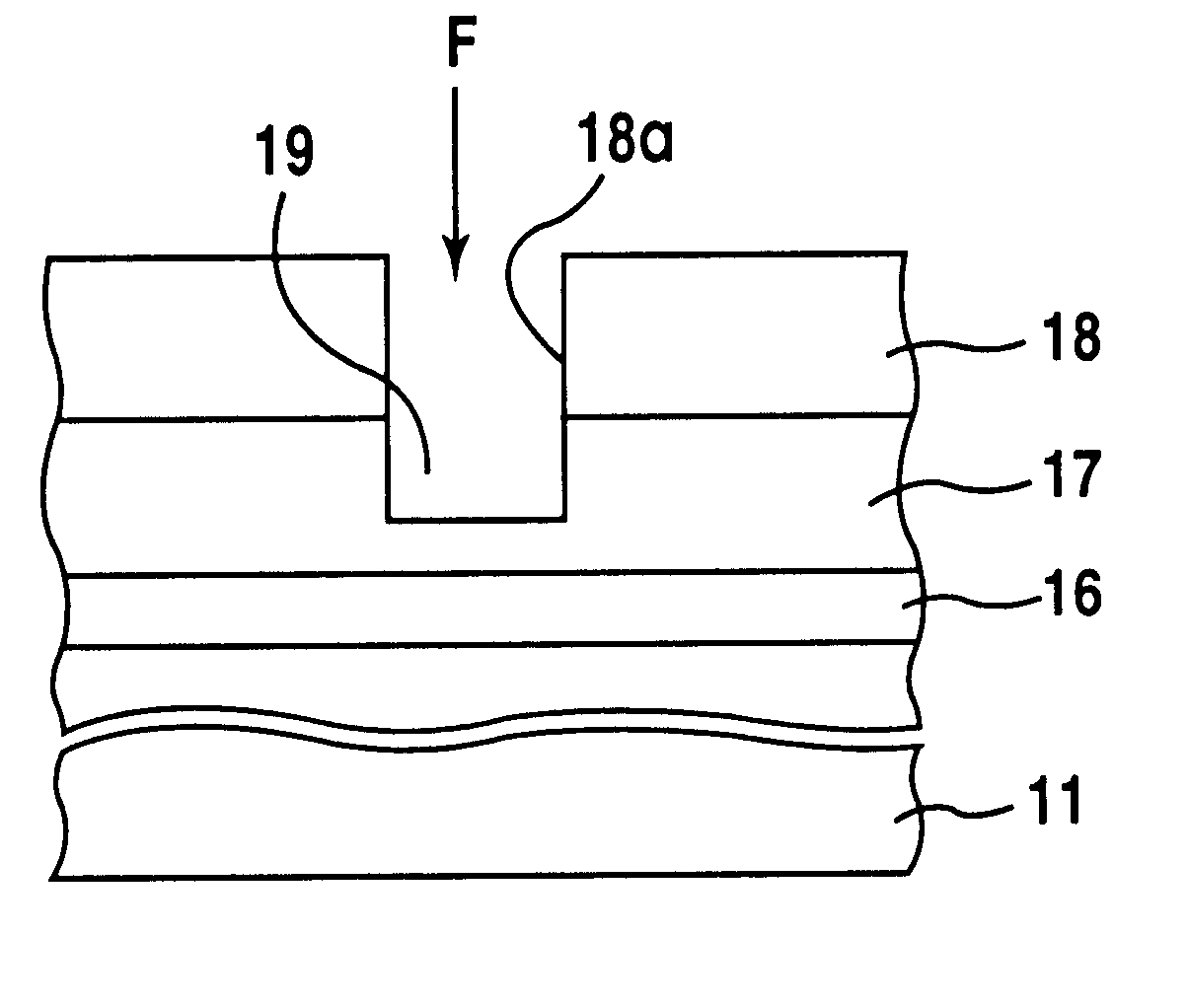
Next, a step of selectively etching the silicon nitride in forming the contact holes by the BLC technique will be explained.

First, steps of forming up to a structure shown in FIG. 16A will be explained.

A groove 52 is formed in the device isolation region of the silicon substrate 51, and then a buried insulating film 53 made of silicon oxide is filled into the groove 52. As a method of filling the buried insulating film 53 into the groove 52, such a method can be employed, for example, that the buried insulating film 53 is formed by CVD in the groove 52 and on the silicon substrate 51 and then the buried insulating film 53 on a surface of the silicon substrate 51 is removed by polishing.

A gate insulating film 54, a gate electrode 55, and a gate covering insulating film 56 are then formed in an active region. Then, low-impurity concentration regions 57s, 57d are formed by ion-implanting the impurity into the silicon substrate 51 on both sides of the gate electrode 55 at a low dosage b...


PUM


Abstract

There are included steps of forming a silicon nitride layer on a silicon layer or a silicon oxide layer, loading the silicon layer or the silicon oxide layer and the silicon nitride layer in a dry etching atmosphere, and selectively etching the silicon nitride layer with respect to the silicon layer or the silicon oxide layer by flowing a fluorine gas consisting of any one of CH2F2, CH3F, or CHF3 and an inert gas to the dry etching atmosphere. Hence, in the etching process of the silicon nitride layer, the etching selectivity of the silicon nitride layer to Si or SiO2 can be enhanced and also etching anisotropy can be enhanced.

Description

1. Field of the InventionThe present invention relates to a method of etching a silicon nitride layer and a method of manufacturing a semiconductor device including a step of patterning the silicon nitride layer.2. Description of the Prior ArtWith the development of miniaturization of the semiconductor integrated circuit (LSI), a SAC (Self Alignment Contact) technique and a BLC (Border Less Contact) technique have been employed to arrange the wirings from an impurity diffusion layer to a field insulating film.According to the SAC technique, in the event that wirings are connected to two MOS transistors which employ one impurity diffusion layer as a common constituent element and the wirings are to be connected to a common impurity diffusion layer between two gate electrodes, connecting positions of the wirings are regulated by an insulating layer formed on surfaces of two gate electrodes.Like the above, with the use of the SAC technique, the wirings can be easily and firmly connecte...

Claims


Application Information

Patent Timeline
IPC IPC(8): H01L21/60H01L21/02H01L21/311H01L21/8242
CPCH01L21/31116H01L21/76897H01L27/10888H01L27/10873H01L27/10855H10B12/05H10B12/485H10B12/0335H01L21/306
Inventor OSHIMA, TADASHI
Owner FUJITSU SEMICON LTD
Why Eureka
Try Eureka