Method of fabricating micro electro mechanical system structure which can be vacuum-packed at wafer level

a micro electro mechanical and wafer-level technology, applied in the direction of instruments, turn-sensitive devices, semiconductor/solid-state device details, etc., can solve the problems of reducing the efficiency of the mechanical system, affecting the completeness of the structure, and affecting the quality of the mechanical system

Inactive Publication Date: 2002-05-21
SAMSUNG ELECTRONICS CO LTD
View PDF17 Cites 140 Cited by
  • Summary
  • Abstract
  • Description
  • Claims
  • Application Information

AI Technical Summary

Benefits of technology

It is a second object of the present invention to provide a method of fabricating a MEMS structure which can be vacuum-packaged at the wafer level.

Problems solved by technology

Here, residual stress existing in the poly silicon has a negative influence on a completed MEMS structure.
Moreover, it is difficult to fabricate a structure having a thickness greater than 10 .mu.m with general polysilicon taking into consideration the fabrication processes that are available.
Although this process can realize a structure which is thick and does not have residual stress, it is difficult to form more than one structure layer.
Consequently, a complex structure cannot be formed through this process.
In the case of bulk micromachining that forms a MEMS structure using single crystalline anisotropic etching, it is difficult to form a structure having a high aspect ratio due to the characteristic of anisotropic etching.
In resonance type gyroscopes among MEMS structures, the Q-factor is vulnerable to the surrounding vacuum level during resonance.
Additionally, it is difficult to apply a general IC / ASIC packaging process to chips having a MEMS structure.
Therefore, it is difficult to realize automization of the fabrication process.

Method used


Image

  • Method of fabricating micro electro mechanical system structure which can be vacuum-packed at wafer level
  • Method of fabricating micro electro mechanical system structure which can be vacuum-packed at wafer level
  • Method of fabricating micro electro mechanical system structure which can be vacuum-packed at wafer level

Examples


Embodiment Construction

Hereinafter, embodiments of a method of fabricating a micro electromechanical system (MEMS) structure according to the present invention will be described in detail with reference to the attached drawings.

An example of a method of fabricating a microgyroscope having a MEMS structure will be described. In particular, a method of forming a vacuum structure at the wafer level will be described.

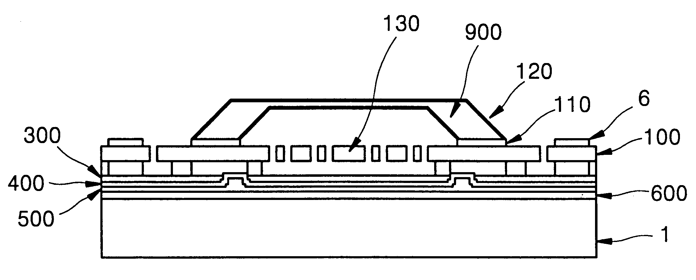
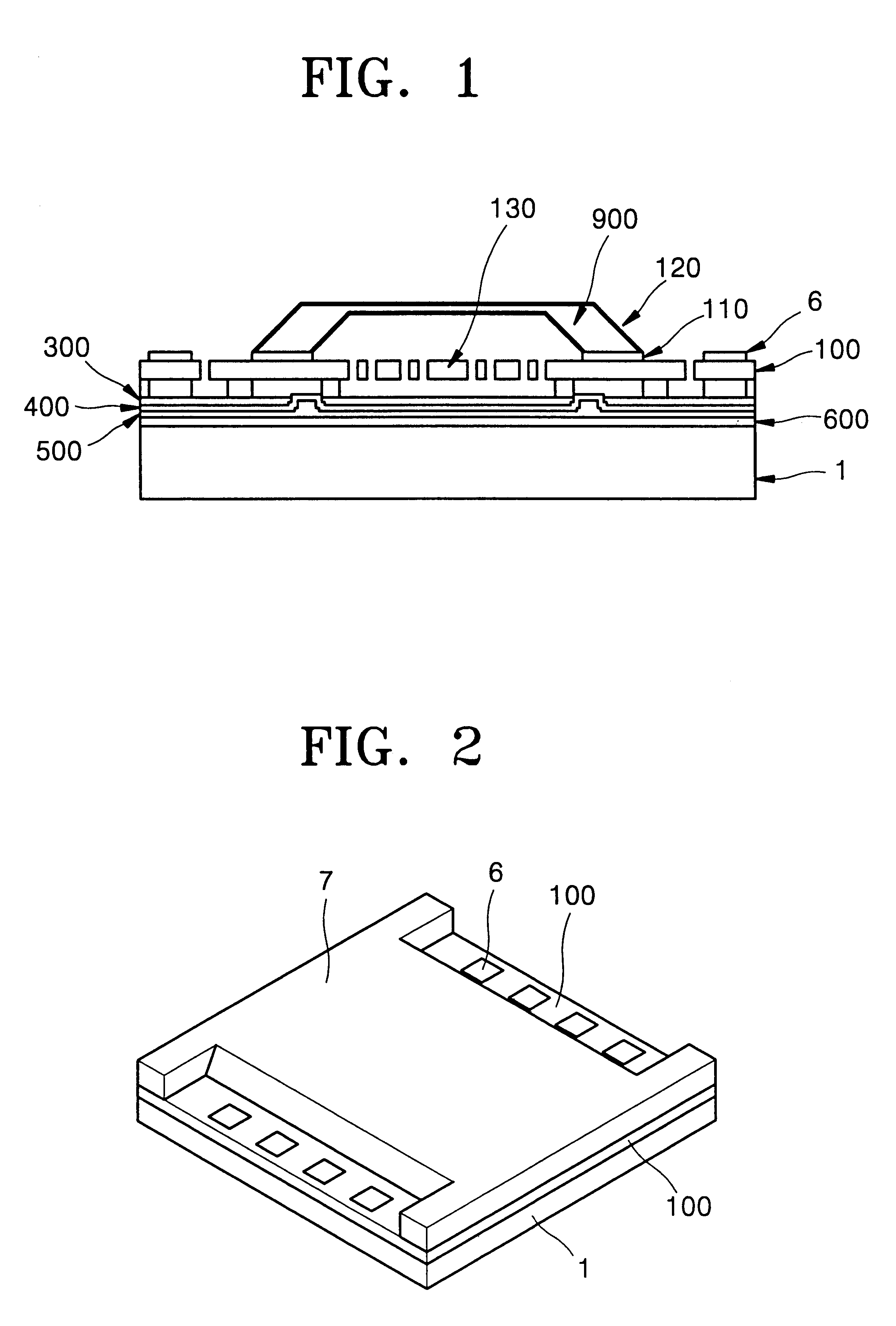
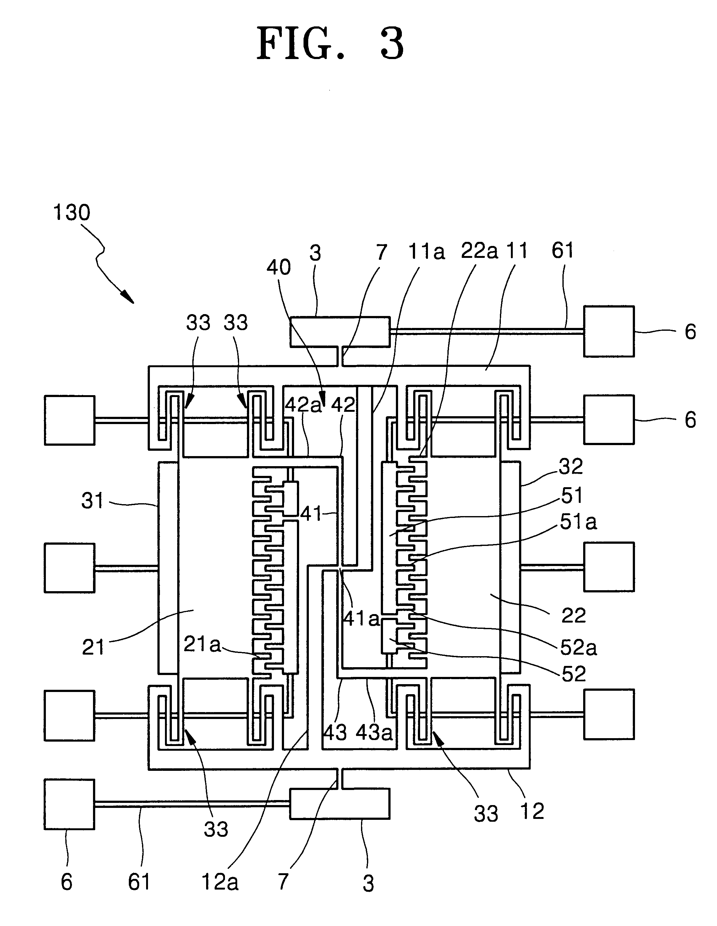
The following description concerns the structure of a microgyroscope fabricated using a completed MEMS structure. FIG. 1 is a schematic cross-sectional view illustrating a completed microgyroscope. FIG. 2 is a schematic perspective view illustrating a microgyroscope. FIG. 3 is a sectional plan view illustrating the internal resonance structure of a microgyroscope. FIG. 4 is a schematic perspective view illustrating the resonance structure of a microgyroscope.

Referring to FIGS. 1 and 2, a resonance structure subjecting to a MEMS structure and pads 6 electrically connected to the resonance structur...


PUM

PropertyMeasurementUnit
thicknessaaaaaaaaaa
thicknessaaaaaaaaaa
temperatureaaaaaaaaaa

Abstract

A method of fabricating a micro electromechanical system (MEMS) structure which can be vacuum-packaged at the wafer level is provided. The method includes the steps of forming a multilayered stack including a signal line on a first wafer; bonding a second wafer to the multilayered stack; polishing the first wafer to a predetermined thickness; forming a MEMS structure in a vacuum area of the first wafer and a pad outside the vacuum area, the MEMS structure and the pad being connected to the signal line; forming a structure in a third wafer to have space corresponding to the vacuum area of the MEMS structure; and bonding the third wafer to the polished surface of the first wafer in a vacuum state. For protection of the structure and maintaining a vacuum level required for operation, the fabricated structure is vacuum-packaged at the wafer level, thereby improving the yield of fabrication. In addition, since a special vacuum packaging process is not necessary, the fabrication can be simplified.

Description

1. Field of the InventionThe present invention relates to a method of fabricating a micro electro mechanical system (MEMS) structure which can be vacuum-packaged at the wafer level.2. Description of the Related ArtIn the case of surface micromachining most widely used in fabricating MEMS structures, polysilicon is used as the material for the structure. Here, residual stress existing in the poly silicon has a negative influence on a completed MEMS structure. Moreover, it is difficult to fabricate a structure having a thickness greater than 10 .mu.m with general polysilicon taking into consideration the fabrication processes that are available. To solve this problem, a process of using SOI or a result obtained by bonding single crystalline silicon to glass to a thickness of 40 .mu.m as a structure layer has been used. Although this process can realize a structure which is thick and does not have residual stress, it is difficult to form more than one structure layer. Consequently, a c...

Claims


Application Information

Patent Timeline
Patent Type & Authority Patents(United States)
IPC IPC(8): B81B3/00B81B7/00G01P15/08G01P1/02G01C19/56G01P1/00H01L23/58B81C3/00G01C19/574G01C19/5769H01L23/02
CPCB81C1/00293G01P15/0802G01P1/02G01C19/5769H01L23/58
Inventor HA, BYEOUNG JUBAEK, SEOG-SOONKIM, HYUN-CHEOLSONG, HOONOH, YONG-SOO
Owner SAMSUNG ELECTRONICS CO LTD
Why Eureka
Try Eureka