Trench-defined silicon germanium ESD diode network

a diode network and silicon germanium technology, applied in the field of microelectronic devices, can solve the problems of affecting device performance, unable to fully or partially operate the device, and difficult to achieve, so as to prevent harmful voltage and current spikes

Inactive Publication Date: 2002-05-28
GLOBALFOUNDRIES US INC
View PDF20 Cites 65 Cited by
  • Summary
  • Abstract
  • Description
  • Claims
  • Application Information

AI Technical Summary

Benefits of technology

is to provide a circuit and network which prevents harmful voltage and current spikes for microelectronic devices.

Problems solved by technology

Both voltage and the current spikes, usually of very short duration, can break down the isolation or diffusions in various portions of individual such devices, thus rendering the device completely or partially inoperable.
Capacitive loading becomes a major concern for microelectronic chips running at RF frequencies, i.e., frequencies greater than 1 GHz, as the capacitive loading of conventional ESD devices has an adverse effect on device performance.
For example, at 1 GHz a capacitance of 1 pF is acceptable, but at 10 GHz the capacitance must be in the order of 0.1 pF, which is difficult to achieve, and for 100 GHz the capacitance would need to be around 0.01 pF, which is very difficult if impossible to achieve with conventional ESD protection circuits.
However, such enlarged ESD pad structures cause detrimental capacitive loading effects which distort frequency and impact chip performance.
Data comparing performance of SiGe devices over wide frequency ranges indicates significant performance degradation for those with ESD protection versus those without.

Method used


Image

  • Trench-defined silicon germanium ESD diode network
  • Trench-defined silicon germanium ESD diode network
  • Trench-defined silicon germanium ESD diode network

Examples


Embodiment Construction

)

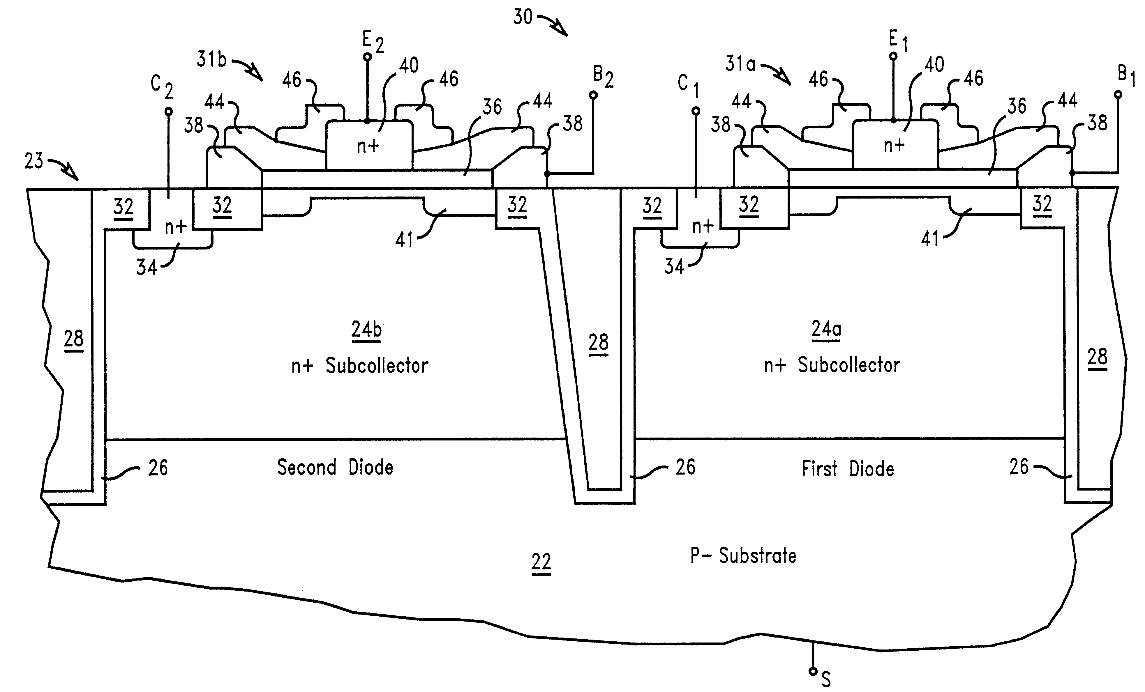
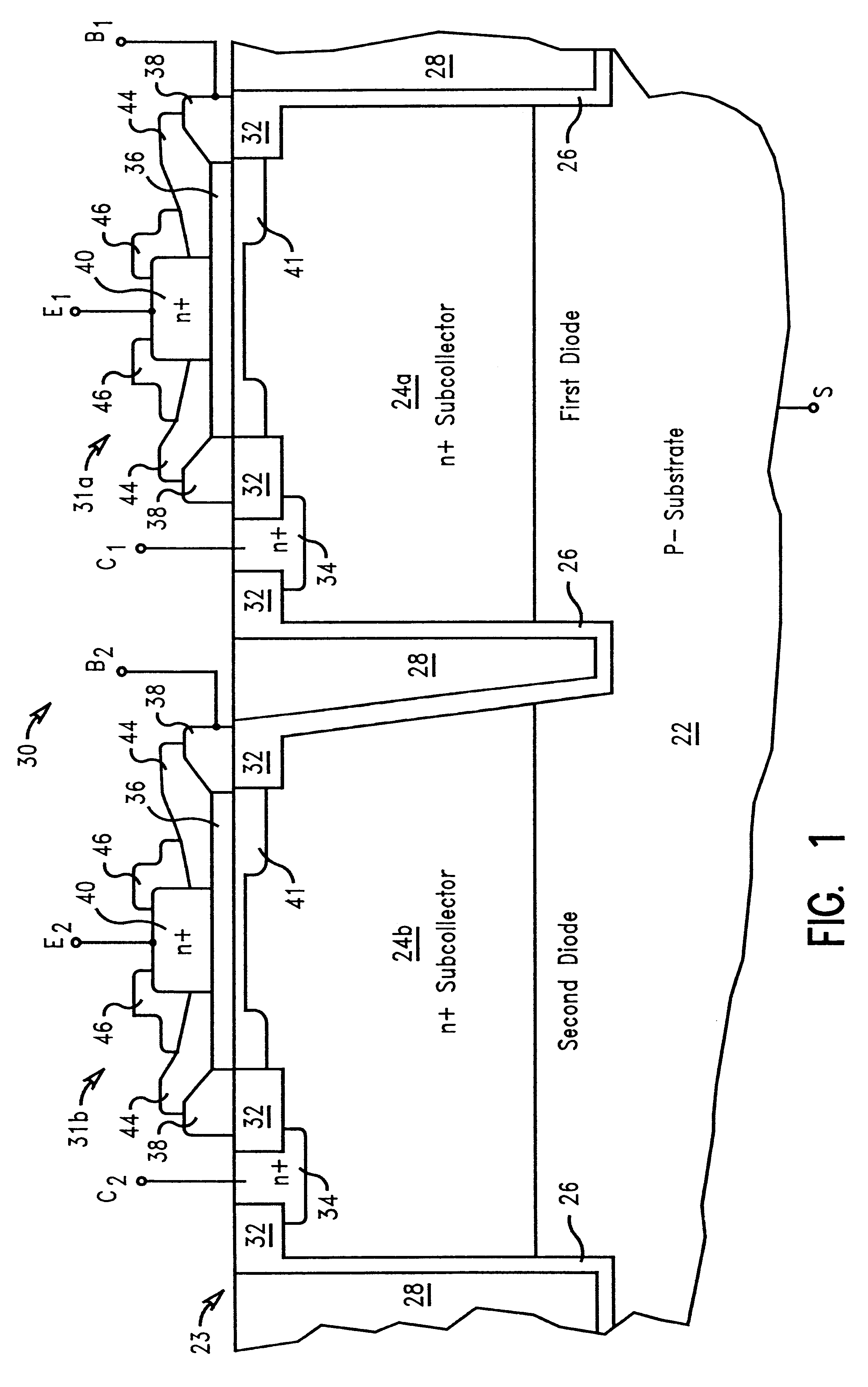
In describing the preferred embodiment of the present invention, reference will be made herein to FIGS. 1-28 of the drawings in which like numerals refer to like features of the invention. Features of the invention are not necessarily shown to scale in the drawings.

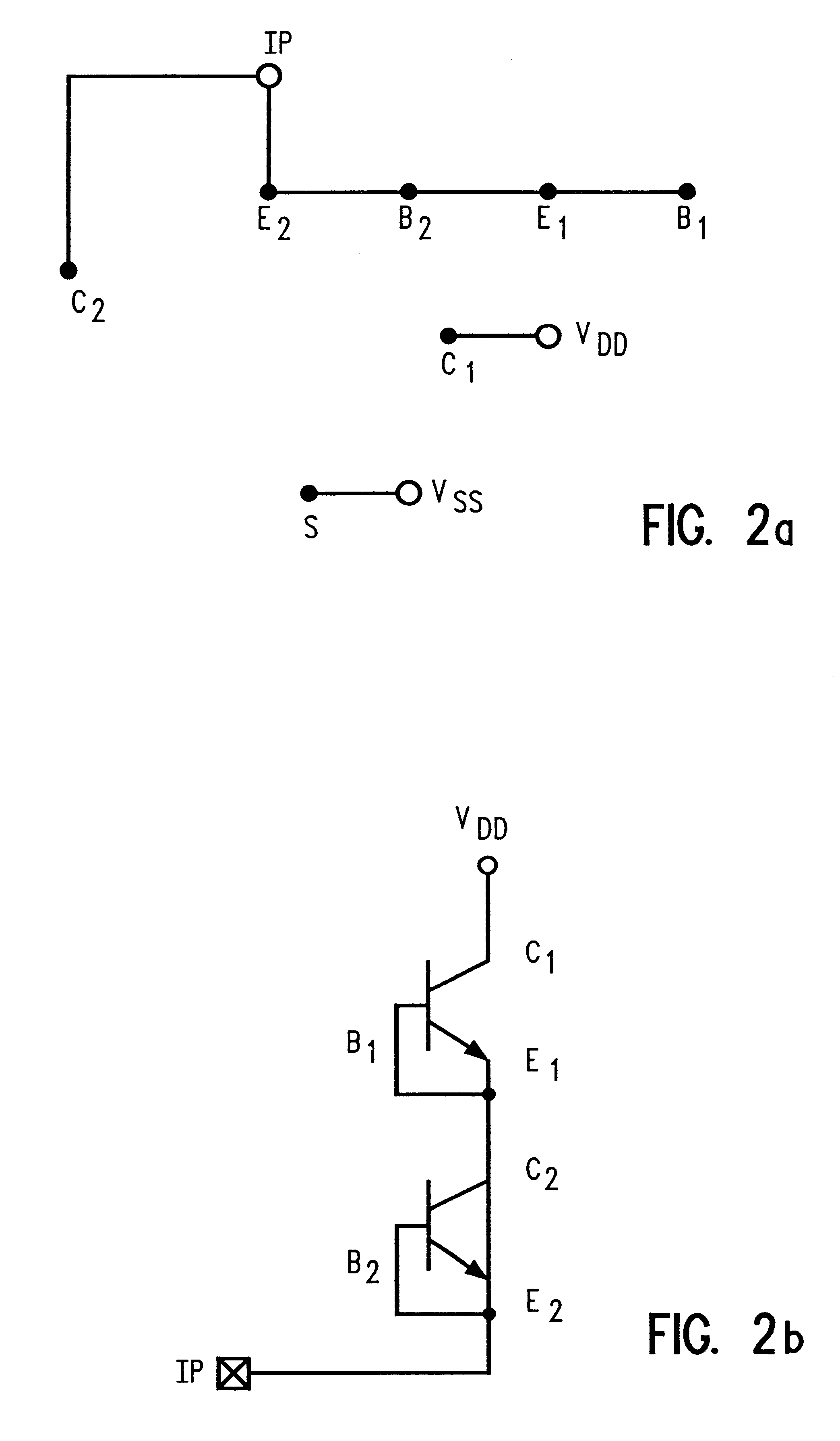
The present invention provides an ESD network which is formed using silicon germanium (SiGe) transistor elements for radio frequency (RF) and mixed signal applications as well as for mixed voltage interface network for digital / analog applications. SiGe heterojunction bipolar transistor (HBT) devices in diode configuration provide ESD protection. Also, SiGe HBT device base-collector or base-emitter junctions provide ESD protection for positive pulses, and SiGe HBT device collector-substrate junctions provide ESD protection for negative pulses. SiGe HBT devices in serial configuration provide ESD protection for mixed signal applications.

FIG. 1 shows an embodiment of the present invention and depicts a diode network 30 whic...


PUM


Abstract

A silicon-germanium ESD element comprises a substrate of a first dopant type coupled to a first voltage terminal and a first diode-configured element. The first diode-configured element has a collector region of a second dopant type in the substrate, a SiGe base layer of the first dopant type on the collector region, with the SiGe base layer including a base contact region, and an emitter of the second dopant type on the SiGe base layer. Preferably, the SiGe base layer ion the collector region is an epitaxial SiGe layer and the second dopant type of the emitter is diffused in to the SiGe base layer. The ESD element of the present invention may further include a second diode-configured element of the same structure as the first diode-configured element, with an isolation region in the substrate separating the first and second diode-configured elements. The first and second diode-configured elements form a diode network. In each of the embodiments, the isolation regions may be disposed adjacent the collector regions of the diode elements and below a portion of the SiGe base layer of the diode elements. The SiGe base layer in the diode elements preferably comprises an active, single crystal layer in a portion directly over the collector region and a polycrystalline layer in portions directly over the isolation regions. The isolation regions may be shallow or deep trench isolations.

Description

1. Field of the InventionThe present invention relates to microelectronic devices and, in particular, to a silicon germanium-based circuit and network configuration to reduce harmful effects of electrostatic discharge in such devices.2. Description of Related ArtElectrostatic discharge (ESD) phenomenon causes high voltage and / or current to be impressed across the terminals of microelectronic and other devices. Both voltage and the current spikes, usually of very short duration, can break down the isolation or diffusions in various portions of individual such devices, thus rendering the device completely or partially inoperable.The energy spectrum as a function of frequency of an ESD event is a function of the ESD phenomenon. There are three models in use to describe ESD: the human body model (HBM), the machine model (MM), and the charge device model (CDM). In the human body model, a 4 KV pulse is assumed with a maximum current of 2.6 amperes with a 150 ns event time. In the 400 volt...

Claims


Application Information

Patent Timeline
Patent Type & Authority Patents(United States)
IPC IPC(8): H01L27/02H05F3/04
CPCH01L27/0255H01L27/0259H01L2924/0002H01L2924/00H05F3/04
Inventor BRENNAN, CIARAN J.HERSHBERGER, DOUGLAS B.LEE, MANKOOSCHMIDT, NICHOLAS T.VOLDMAN, STEVEN H.
Owner GLOBALFOUNDRIES US INC
Why Eureka
Try Eureka