Electrooptical apparatus, method of producing the same and electronic apparatus

a technology of electronic equipment and scanning lines, applied in the field of electronic equipment, can solve the problems of not being able to produce wirings for all image signal lines, lines peeling, and currently available techniques for forming scanning lines of thin metal films

Inactive Publication Date: 2002-08-13
SEIKO EPSON CORP
View PDF9 Cites 77 Cited by
  • Summary
  • Abstract
  • Description
  • Claims
  • Application Information

AI Technical Summary

Problems solved by technology

On the other hand, there are no currently available techniques which can be used to form the scanning lines of a thin metal film or a thin metal silicide film, because existing techniques would be subject to the problem that the sca...

Method used


Image

  • Electrooptical apparatus, method of producing the same and electronic apparatus
  • Electrooptical apparatus, method of producing the same and electronic apparatus
  • Electrooptical apparatus, method of producing the same and electronic apparatus

Examples


Embodiment Construction

Referring to the drawings, embodiments of the invention are described below. In the embodiments described below, a liquid crystal apparatus is taken as an example of an electrooptical apparatus according to the invention.

Construction and Operation of Liquid Crystal Apparatus

Referring to FIGS. 1 to 10, the construction and the operation of a liquid crystal apparatus according to an embodiment of the invention are described below.

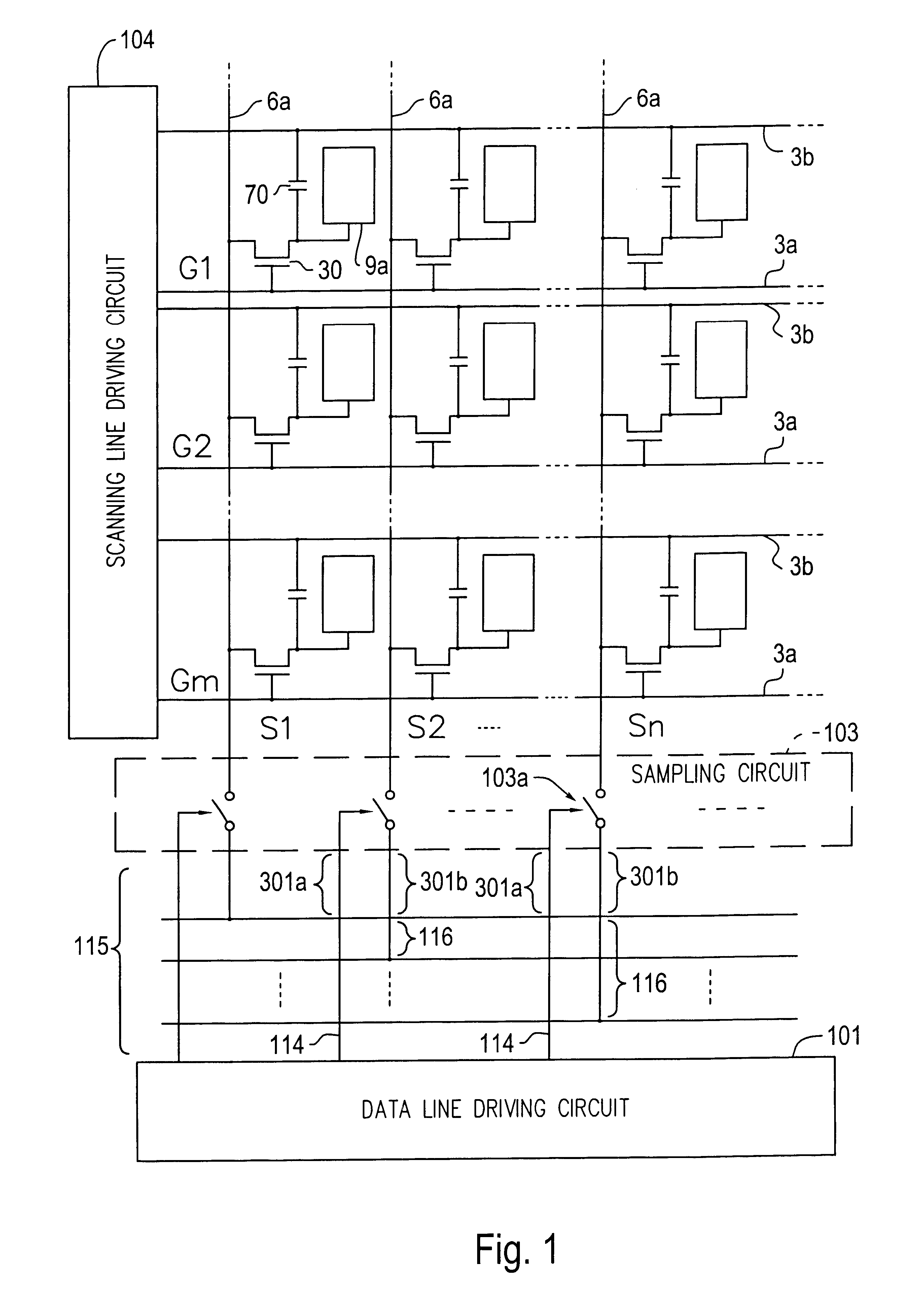
First, the circuit configuration of the liquid crystal apparatus is described with reference to the schematic shown in FIG. 1.

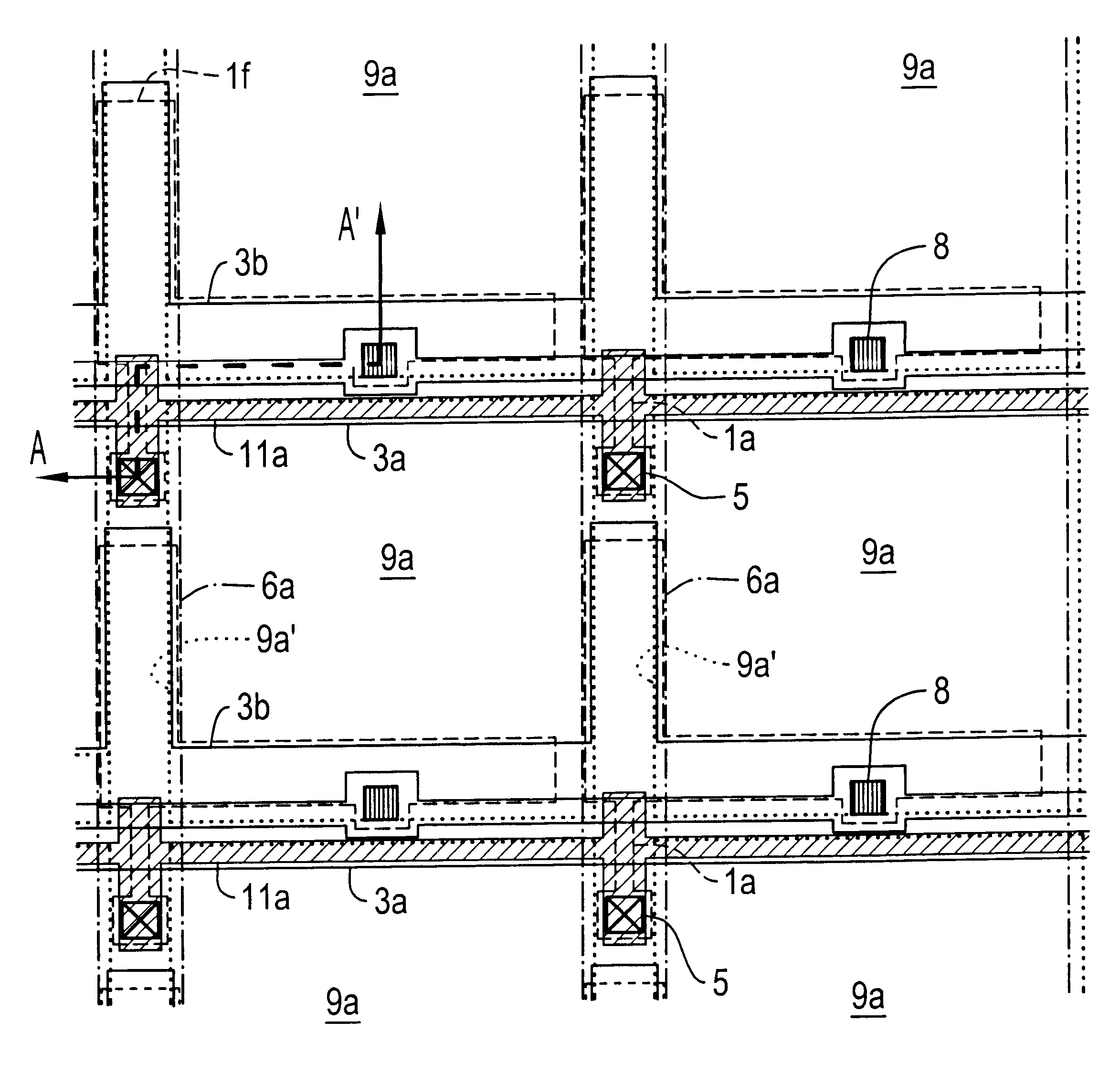
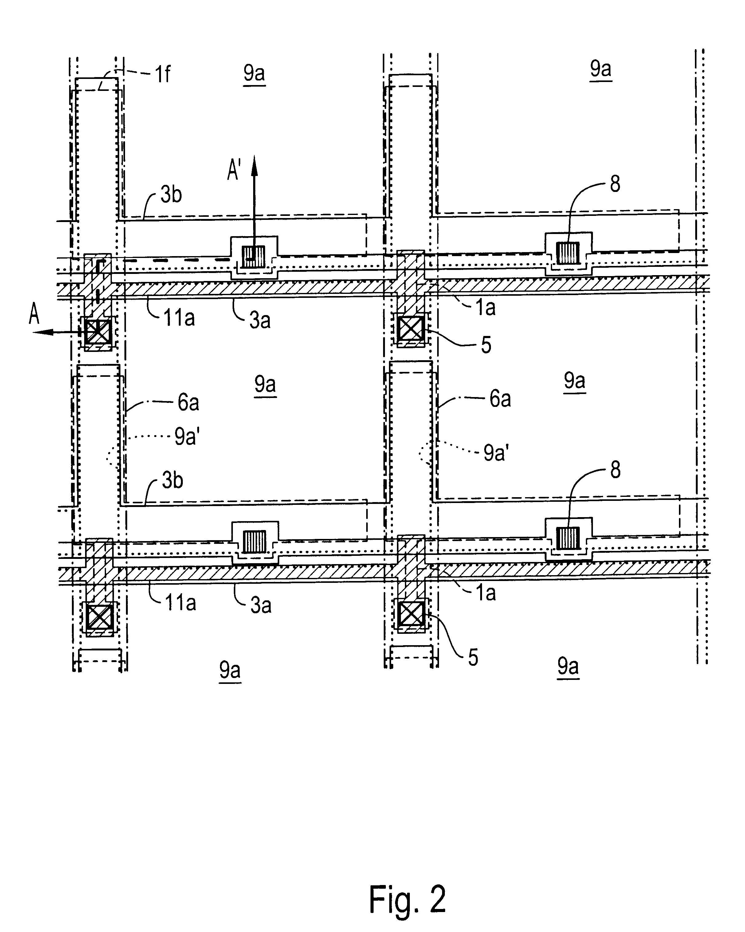
FIG. 1 illustrates an equivalent circuit of wirings and various other elements in a plurality of pixels formed in an array fashion in an image displaying area on an TFT array substrate of the liquid crystal apparatus, and also illustrates peripheral circuits disposed in a peripheral area outside the image displaying area.

In the present embodiment, as shown in FIG. 1, a plurality of pixels are arranged in a matrix fashion in the image d...


PUM


Abstract

The invention provides an electrooptical apparatus, such as a liquid crystal apparatus, including a built-in-peripheral circuit in which the resistance of input/output wirings in the peripheral circuit is reduced by effectively using thin films forming pixels, thereby making it possible to display a high-quality image. The liquid crystal apparatus includes a liquid crystal layer disposed between a pair of substrates and pixel electrodes formed in a matrix fashion on a TFT array substrate. A light blocking film made of refractory metal is provided under TFTs of respective pixels, scanning lines, and capacitance lines. There are also provided peripheral wirings, such as image signal lines including second wiring made of the same metal film as that of the data lines and also including first wiring whose layers are conductive film as that of the light blocking film and the same polysilicon film as that of the scanning lines, respectively.

Description

1. Field of the InventionThe present invention relates to an electrooptical apparatus such as an active matrix liquid crystal apparatus driven by thin-film transistors (hereinafter also referred to as TFTs), and also to a method of producing such an electrooptical apparatus. More particularly, the present invention relates to an electrooptical apparatus such as a liquid crystal apparatus suitable for use in a liquid crystal projector, and including peripheral circuits such as a data line driving circuit and a scanning line driving circuit, wherein a light blocking film is disposed under each TFT. The present invention further relates to a method of producing such an electrooptical apparatus.2. Description of Related ArtIn conventional liquid crystal apparatus having built-in peripheral circuits, peripheral circuits such as a data line driving circuit, a scanning line driving circuit, and a sampling circuit are formed on a TFT array substrate, which is one of two substrates between w...

Claims


Application Information

Patent Timeline
IPC IPC(8): G02F1/13G02F1/1362G09G3/36G02F1/1333
CPCG02F1/13454G02F1/136209G09G3/3648H01L29/78633G02F1/1333G09G2320/0223H01L27/124G02F1/136227
Inventor MURADE, MASAO
Owner SEIKO EPSON CORP
Why Eureka
Try Eureka